Ultraviolet laser ablative patterning of microstructures in semiconductors

a technology of ultraviolet laser and microstructure, which is applied in the direction of manufacturing tools, metal working equipment, welding/soldering/cutting articles, etc., can solve the problems of significant problems encountered in laser dicing processes, holes that are unsuitable for further processing, and holes that are typically observed to be marred, etc., to reduce damage or marring of processed semiconductor workpieces, improve the aspect ratio, and the effect of greater depth

Inactive Publication Date: 2007-01-02
ELECTRO SCI IND INC
View PDF46 Cites 51 Cited by
  • Summary
  • Abstract
  • Description
  • Claims
  • Application Information

AI Technical Summary

Benefits of technology

[0017]An advantage of using UV wavelengths is the capability of producing spot sizes significantly smaller than those achievable with longer wavelength sources. This small spot size capability enables the production of micron-scale feature sizes in silicon. Also, for a fixed spot size achievable with conventional Gaussian focusing techniques, a shorter wavelength allows for formation of features with improved aspect ratios due to the greater depth of focus afforded at ultraviolet wavelengths.
[0018]The present invention also provides methods for reducing damage or marring of processed semiconductor workpieces resulting from stray reflections of the ultraviolet processing beam from workpiece supporting structures, such as wafer chucks, by use of substantially nonreflecting materials and novel fabrication techniques for workpiece supporting structures.

Problems solved by technology

However, since silicon is a weak absorber at 1064 nm, significant problems have been encountered in laser dicing processes operating at or near this wavelength.
The cut quality is typically observed to be marred by redeposition of silicon along the wafer surface and along the walls of the cut.
This apparent redeposition of silicon made the holes unsuitable for further processing.
He teaches that the primary cause for poor cut quality resulting from redeposition when employing near infrared lasers is use of laser pulsewidths exceeding about 1 ns.
Dahm also mentions that near infrared lasers, such as 1064 nm Nd:YAG lasers, are used for high speed applications because of their ability to produce greater power than UV lasers, arguing that UV lasers cannot develop sufficient power to process silicon at high speeds.

Method used


Image

  • Ultraviolet laser ablative patterning of microstructures in semiconductors
  • Ultraviolet laser ablative patterning of microstructures in semiconductors
  • Ultraviolet laser ablative patterning of microstructures in semiconductors

Examples


Embodiment Construction

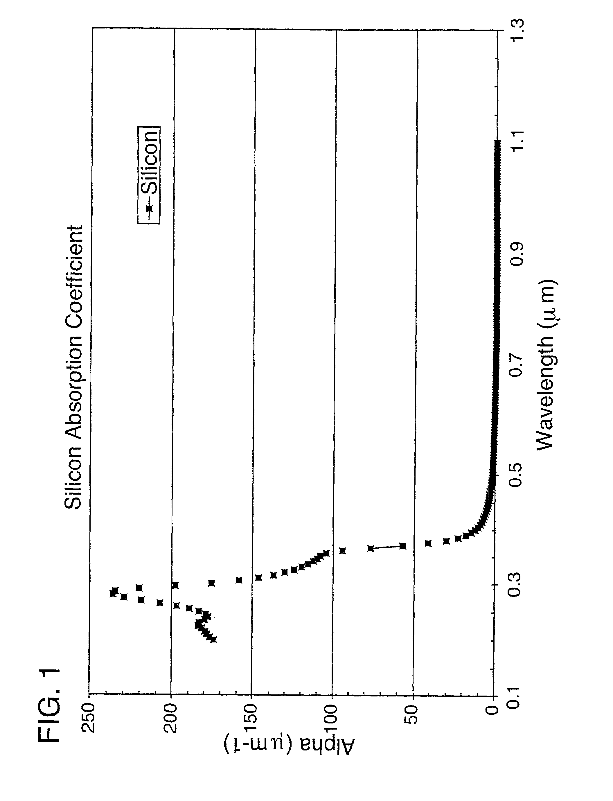
[0033]FIG. 1 displays the optical absorption coefficient of silicon as a function of wavelength. With reference to FIG. 1, silicon exhibits a very sharp rise in the optical absorption at wavelengths in the ultraviolet. The present invention advantageously utilizes laser wavelengths shorter than 390 nm and takes advantage of the increased absorption of silicon in the ultraviolet to efficiently ablate silicon and thereby form a variety of useful patterns or features directly in silicon. The absorption behavior facilitates strongly ablative removal of silicon in the ultraviolet with a greatly reduced thermally affected zone in comparison with features formed using either 532 nm or 1064 nm pulsed output as taught by the prior art.

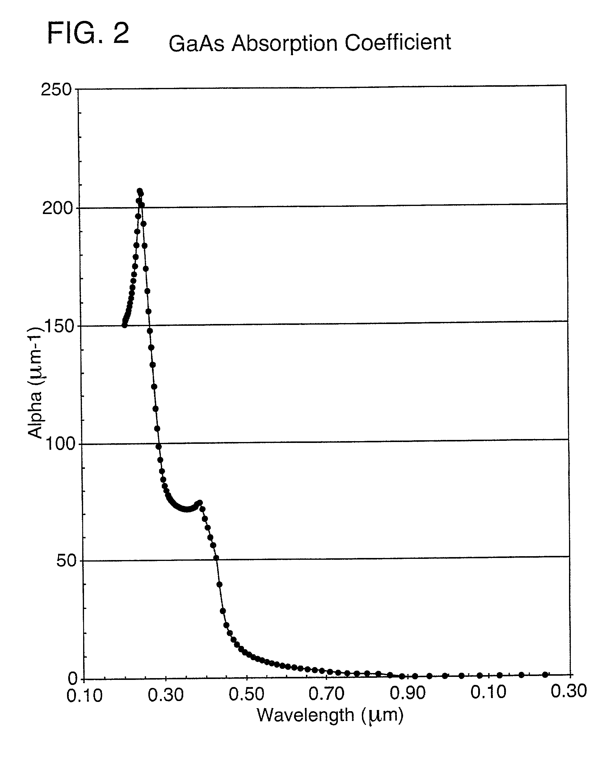
[0034]FIG. 2 displays the optical absorption coefficient of GaAs as a function of wavelength. With reference to FIG. 2, GaAs exhibits a very sharp rise in the optical absorption at wavelengths in the ultraviolet. The absorption coefficient at 355 nm of GaAs and...


PUM

PropertyMeasurementUnit
wavelengthaaaaaaaaaa
thickaaaaaaaaaa
bite sizeaaaaaaaaaa

Abstract

Patterns with feature sizes of less than 50 microns are rapidly formed directly in semiconductors, particularly silicon, GaAs, indium phosphide, or single crystalline sapphire, using ultraviolet laser ablation. These patterns include very high aspect ratio cylindrical through-hole openings for integrated circuit connections; singulation of processed die contained on semiconductor wafers; and microtab cutting to separate microcircuit workpieces from a parent semiconductor wafer. Laser output pulses (32) from a diode-pumped, Q-switched frequency-tripled Nd:YAG, Nd:YVO4, or Nd:YLF is directed to the workpiece (12) with high speed precision using a compound beam positioner. The optical system produces a Gaussian spot size, or top hat beam profile, of about 10 microns. The pulse energy used for high-speed ablative processing of semiconductors using this focused spot size is greater than 200 μJ per pulse at pulse repetition frequencies greater than 5 kHz and preferably above 15 kHz. The laser pulsewidth measured at the full width half-maximum points is preferably less than 80 ns.

Description

RELATED APPLICATIONS[0001]This patent application derives priority from U.S. Provisional Application No. 60 / 265,556, filed Jan. 31, 2001, from U.S. Provisional Application No. 60 / 297,218, filed Jun. 8, 2001, is a division of U.S. patent application Ser. No. 09 / 957,633, filed Sep. 19, 2001 (now abandoned), which claims priority from U.S. Provisional Application No. 60 / 233,914, filed Sep. 20, 2000, and is a division of U.S. patent application Ser. No. 09 / 803,382, filed Mar. 9, 2001 (now abandoned), which claims priority from U.S. Provisional Application No. 60 / 233,913, filed Sep. 20, 2000.TECHNICAL FIELD[0002]This invention relates to a method and / or apparatus for high-speed formation of micron-scale features by ablation of semiconductors, and particularly silicon, using pulsed output of an ultraviolet (UV) laser.BACKGROUND OF THE INVENTION[0003]The semiconductor industry utilizes numerous techniques to separate distinct electronic devices, often referred to as die, from the semicondu...

Claims


Application Information

Patent Timeline
Patent Type & Authority Patents(United States)
IPC IPC(8): B23K26/38B23K26/04B23K101/40C04B41/91H01L21/301
CPCB23K26/063B23K26/0656B23K26/083B23K26/367B23K26/4075B23K26/0869B23K2201/40B23K26/364B23K26/0622B23K26/066B23K26/40B23K2101/40B23K2103/50B23K26/38B23K26/04
Inventor BAIRD, BRIAN W.WOLFE, MICHAEL J.HARRIS, RICHARD S.FAHEY, KEVIN P.ZOU, LIAN-CHENGMCNEIL, THOMAS R.
Owner ELECTRO SCI IND INC
Why Eureka
Try Eureka