Optical information recording medium, method for manufacturing the same and recording/reproduction method
- Summary
- Abstract
- Description
- Claims
- Application Information
AI Technical Summary
Benefits of technology
Problems solved by technology
Method used
Image
Examples
working examples
[0051]The following is a more detailed explanation of the present invention, with reference to specific working examples.
working example 1
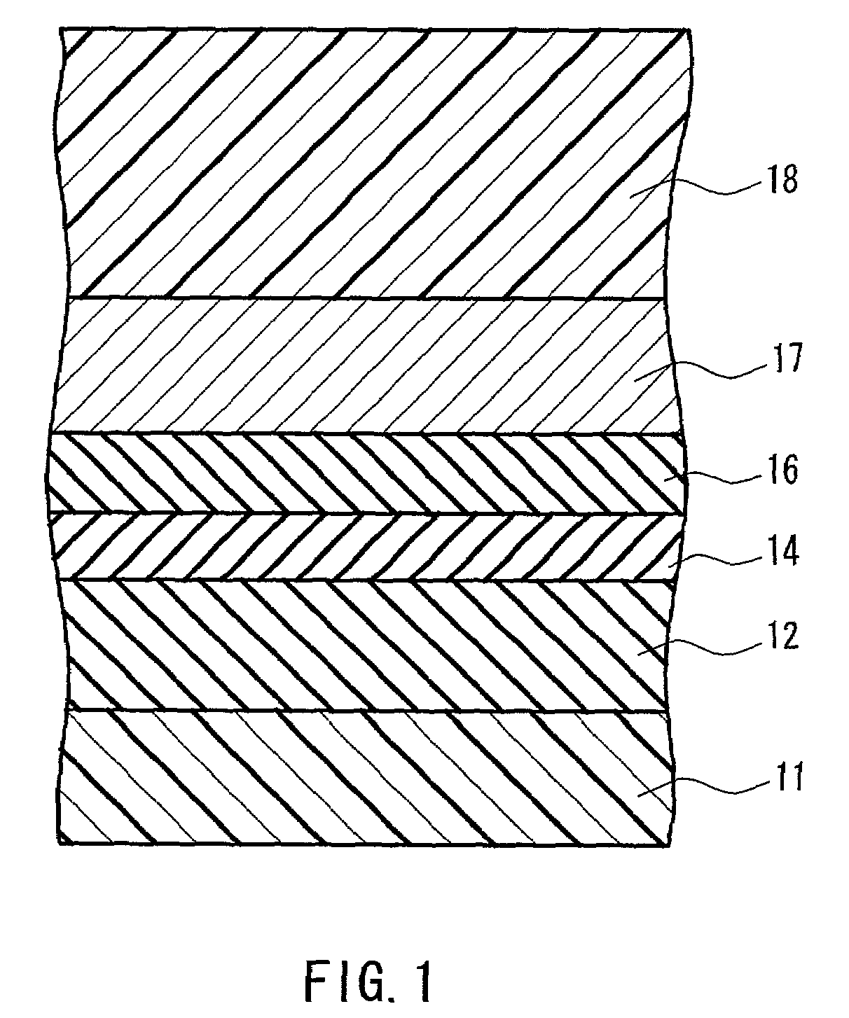
[0052]Referring to FIG. 1, the structure of a disk using this working example is explained. Dielectric layers, recording layer and reflective layer were formed by an ordinary thin film forming method (sputtering) on a transparent resin disk substrate 11. A first dielectric layer 12, a recording layer 14, a second dielectric layer 16 and a reflective layer 17 are provided in that order on the disk substrate 11. On top of that, a closely adhered protective layer 18 was provided
[0053]In this working example, a polycarbonate substrate was used for the substrate 11. Moreover, the disk substrate that was used had groove-shaped protrusions / recessions for tracking in its surface.
[0054]Using a UV curing resin (adhesive), a polycarbonate substrate was adhered as the protective layer 18 on the films layered by film formation on the substrate 11.
[0055]The following explains the results of observing the Ag corrosion after a high-temperature high-humidity test when using an oxide or a nitrooxide ...
working example 2
[0068]The following is an explanation of a signal amplitude evaluation when using an oxide or nitrooxide of Ta in the disk of Working Example 1.
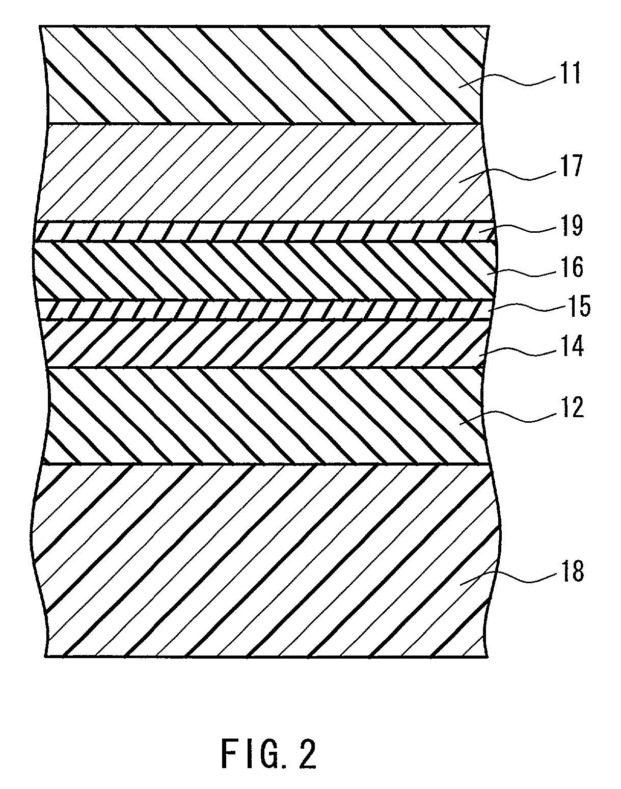
[0069]The disk configuration used in this working example was the same as for Working Example 1.
[0070]The recording and reproduction properties of the disks were evaluated with the following method: To record and reproduce a signal on the optical disks, a laser with a wavelength of 400 nm and a NA of 0.65 was used. As the recorded signals, marks with a shortest mark length (3T marks) of 0.26 μm were recorded in the groove portions at a linear velocity of 8.6 m / s and suitable laser power by 8–16 modulation, and the signal amplitude was measured. Table 2 lists the resulting signal amplitudes.
[0071]
TABLE 2second dielectric layersignal amplitude(1) ZnS—SiO2−30.5 dBm(2) Ta oxide−29.2 dBm(3) Ta nitrooxide−29.5 dBm
[0072]According to Table 2, it was found that when using an oxide of Ta or a nitrooxide of Ta as in the present invention, the signal am...
PUM
| Property | Measurement | Unit |
|---|---|---|
| Thickness | aaaaa | aaaaa |
| Thickness | aaaaa | aaaaa |
| Nanoscale particle size | aaaaa | aaaaa |
Abstract
Description
Claims
Application Information
 - R&D
- Intellectual Property
- Life Sciences
- Materials
- Tech Scout
- Unparalleled Data Quality
- Higher Quality Content
- 60% Fewer Hallucinations
Browse by: Latest US Patents, China's latest patents, Technical Efficacy Thesaurus, Application Domain, Technology Topic, Popular Technical Reports.
© 2025 PatSnap. All rights reserved.Legal|Privacy policy|Modern Slavery Act Transparency Statement|Sitemap|About US| Contact US: help@patsnap.com


