Semiconductor device having a crystalline semiconductor film

a technology of crystalline semiconductor and semiconductor film, which is applied in the direction of semiconductor devices, electrical devices, transistors, etc., can solve the problems of difficult circuit formation of such circuits, and achieve the effect of superior characteristics

Inactive Publication Date: 2007-02-06
SEMICON ENERGY LAB CO LTD
View PDF257 Cites 32 Cited by
  • Summary
  • Abstract
  • Description
  • Claims
  • Application Information

AI Technical Summary

Benefits of technology

[0026]The above-mentioned aspect of the invention defines the relationship between the direction in which the crystal structure has continuity and the direction connecting the source and drain regions of a thin-film transistor. To attain a high-speed operation, it is desired that the direction in which the crystal structure has continuity coincide or substantially coincide with the direction connecting the source and drain regions. This provides a configuration in which carriers can move most easily.
[0048]The lower limit depends upon a pressure at which the annealing is performed and a vapor pressure of the halogen compound of the material to be gettered. That is, when the vapor pressure of the halogen compound is smaller than the pressure of the annealing atmosphere, the gettering efficiency is not so high. For example, the vapor pressure of nickel chloride is 38.9 mmHg at 541° C. and 820.6 mmHg at 994° C. Accordingly, when the annealing is performed at the atmospheric pressure (760 mmHg), the effect of the gettering is significantly increased when the temperature is 994° C.

Problems solved by technology

Therefore, it is very difficult to constitute such circuits by using high-temperature polysilicon TFTs or low-temperature polysilicon TFTs as long as they are formed by the current manufacturing techniques.

Method used


Image

  • Semiconductor device having a crystalline semiconductor film
  • Semiconductor device having a crystalline semiconductor film
  • Semiconductor device having a crystalline semiconductor film

Examples


embodiment 1

[0064]This embodiment is directed to a method of effecting crystal growth parallel with a substrate (called “lateral growth”) by selectively introducing into an amorphous silicon film a metal element that accelerates crystallization of silicon.

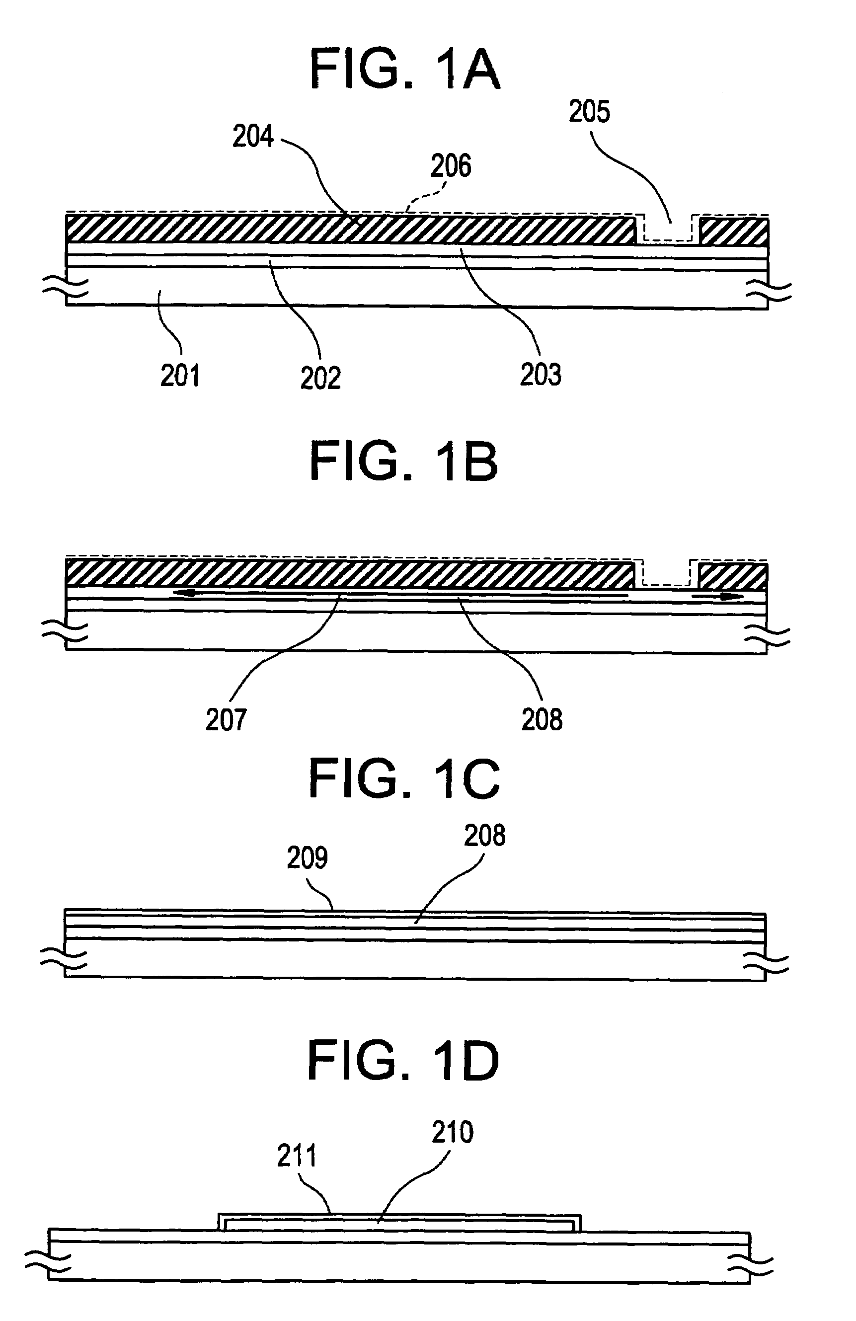
[0065]FIGS. 1A–1D and FIGS. 2A–2E show a manufacturing process according to this embodiment. First, a 3,000-Å-thick silicon oxide film as an undercoat film 202 is formed on a quartz substrate 201. The undercoat film 202 can be omitted if the quartz substrate 201 is sufficiently smooth and if sufficient cleaning is performed.

[0066]Although the use of a quartz substrate is preferable at present, the invention is not limited to the use of a quartz substrate and other substrates can also be used as long as they withstand a heat treatment temperature.

[0067]Next, a 600-Å-thick amorphous silicon film 203 as a starting film of a crystalline silicon film is formed by low-pressure thermal CVD. It is preferred that the amorphous silicon film 203 be thinn...

embodiment 2

[0113]This embodiment is directed to a case where the gate insulating film forming method is modified in the manufacturing method of the first embodiment.

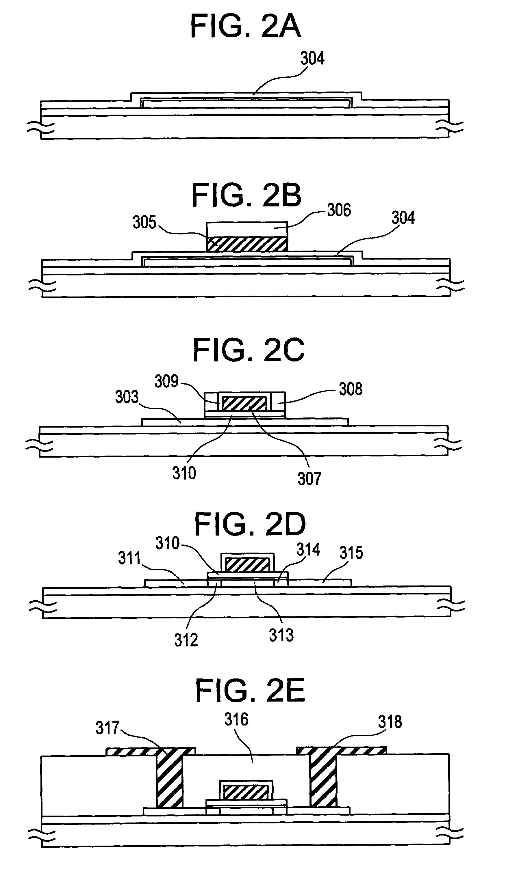
[0114]FIGS. 3A–3D show a manufacturing method according to this embodiment. A crystalline silicon film 208 having a lateral growth region is formed by the steps of FIGS. 1A and 1B. The thickness of an amorphous silicon film as a starting film is set at 500 Å.

[0115]Once the crystalline silicon film 208 is formed, a 200-Å-thick thermal oxidation film 209 is formed by performing a heat treatment of 950° C. for 30 minutes or more by an electrical furnace in an oxygen atmosphere containing HCl at 3%. (FIG. 3A)

[0116]After the thermal oxidation film 209 is removed, the crystalline silicon film 208 is patterned into a pattern 210 which will become a TFT active layer. (FIG. 3B)

[0117]Next, a 1,000-Å-thick gate insulating film 304 is formed by plasma CVD. (FIG. 3C)

[0118]A 300-Å-thick thermal oxidation film 211 is then formed by a heat treatme...

embodiment 3

[0122]This embodiment is directed to a manufacturing method of an active matrix circuit region of an active matrix liquid crystal display device.

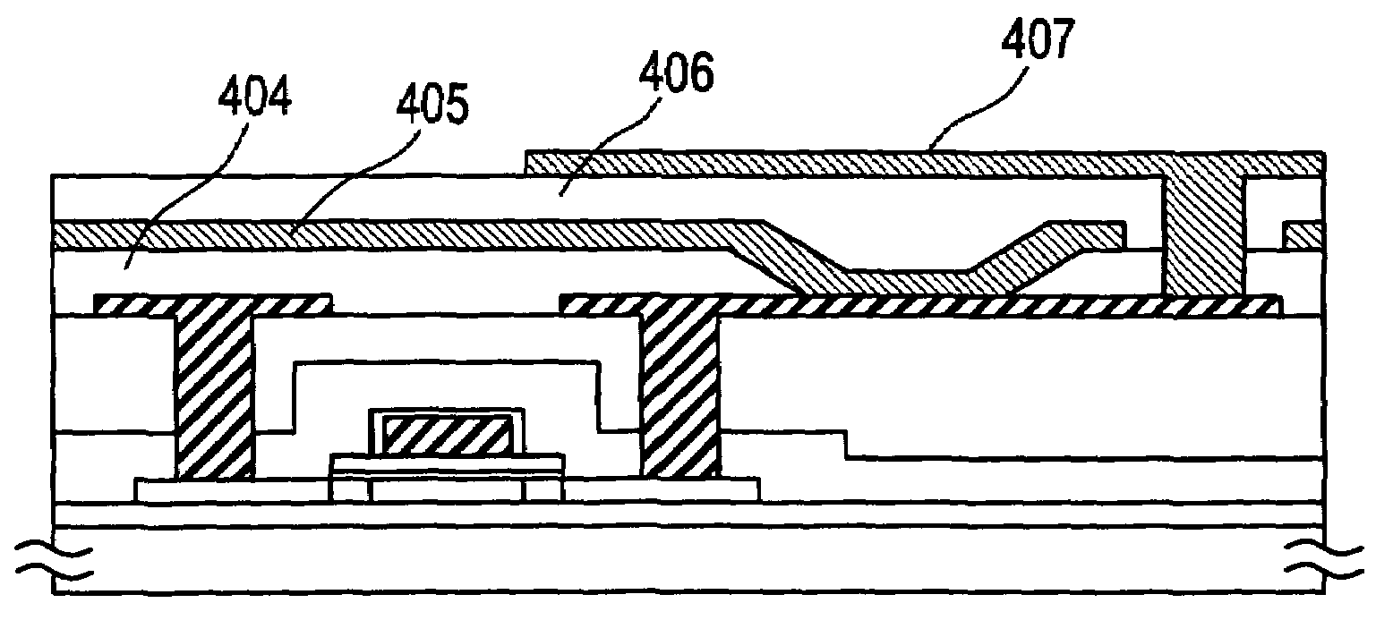
[0123]FIGS. 4A–4D show a manufacturing process according to this embodiment. First, the state of FIG. 2D (also shown in FIG. 4A) is obtained by the process of the first embodiment.

[0124]Next, a 2,000-Å-thick silicon nitride film 401 as a first interlayer insulating film is formed by plasma CVD. A polyimide resin film 402 is formed thereon by spin coating, to obtain the state of FIG. 4B. Resin materials other than polyimide, such as polyamide, polyimideamide and acrylic resin, may also be used.

[0125]After contact holes are formed so as to reach the source region 311 and the drain region 315, a source electrode 403 and a drain electrode 403 are formed each of which is a laminate film of a titanium film, an aluminum film, and a titanium film. The source electrode 403 is so formed as to extend from a source line. (FIG. 4C)

[0126]Part of the sour...


PUM

PropertyMeasurementUnit
temperatureaaaaaaaaaa
frequencyaaaaaaaaaa
angleaaaaaaaaaa

Abstract

Nickel is selectively held in contact with a particular region of an amorphous silicon film. Crystal growth parallel with a substrate is effected by performing a heat treatment. A thermal oxidation film is formed by performing a heat treatment in an oxidizing atmosphere containing a halogen element. During this step, the crystallinity is improved and the gettering of nickel elements proceeds. A thin-film transistor is formed so that the direction connecting source and drain regions coincides with the above crystal growth direction. As a result, a TFT having superior characteristics such as a mobility larger than 200 cm2 / Vs and an S value smaller than 100 mV / dec. can be obtained.

Description

BACKGROUND OF THE INVENTION[0001]1. Field of the Invention[0002]The present invention relates to a crystalline thin-film semiconductor and a manufacturing method thereof. The invention also relates to a semiconductor device using the above thin-film semiconductor and a manufacturing method thereof.[0003]2. Description of Related Art[0004]Techniques are known in which a crystalline silicon film is formed on a glass or quartz substrate and thin-film transistors (hereinafter referred to as TFTs) are formed by using the silicon film. Such TFTs are called high-temperature polysilicon TFTs or low-temperature polysilicon TFTs.[0005]In the case of high-temperature polysilicon TFTs, a crystalline silicon film is formed by a technique including a heat treatment at a relatively high temperature of 800–900° C. It can be said that this technique is derived from an IC manufacturing process using a single crystal silicon wafer. Naturally, high-temperature polysilicon TFTs are formed on a quartz su...

Claims


Application Information

Patent Timeline
Patent Type & Authority Patents(United States)
IPC IPC(8): H01L29/04H01L31/036H01L21/02H01L21/20H01L21/28H01L21/322H01L21/324H01L21/336H01L21/77H01L21/84H01L27/12H01L29/49H01L29/786
CPCH01L21/0242H01L29/78675H01L21/02532H01L21/02667H01L21/02672H01L21/02686H01L21/28158H01L21/3221H01L21/3226H01L29/04H01L29/66757H01L29/66765H01L29/78621H01L21/02488H01L29/4908
Inventor YAMAZAKI, SHUNPEITERAMOTO, SATOSHIKOYAMA, JUNOGATA, YASUSHIHAYAKAWA, MASAHIKOOSAME, MITSUAKIOHTANI, HISASHIHAMATANI, TOSHIJI
Owner SEMICON ENERGY LAB CO LTD
Why Eureka
Try Eureka