Laser diode having an active layer containing N and operable in a 0.6 μm wavelength band

a laser diode and active layer technology, applied in the direction of semiconductor lasers, crystal growth process, polycrystalline material growth, etc., can solve the problems of poor temperature characteristic of the laser diode, poor confinement of carriers, especially electrons, in the active layer, etc., and achieve the effect of facilitating the iii–v compound semiconductor layer

Inactive Publication Date: 2007-04-03
RICOH KK
View PDF18 Cites 33 Cited by
  • Summary
  • Abstract
  • Description
  • Claims
  • Application Information

AI Technical Summary

Benefits of technology

[0011]Accordingly, it is a general object of the present invention to provide a novel and useful laser diode operable in the 600 nm wavelength band wherein the problems are eliminated.
[0021]According to the present invention, a large band discontinuity is guaranteed at the interface between the active layer and the first or second cladding layer as a result of the use of GaInNP for the active layer, and the efficiency of carrier confinement is improved substantially. By adjusting the amount of N in the GaInNP active layer, it becomes possible to set the band offset at the interface between the active layer and the first or second cladding layer as desired. Thereby, the laser diode shows an excellent temperature characteristic and operates stably at the room temperature environment. Further, as a result of the use of GaInNP for the active layer, the laser diode operates in the visible wavelength band including the 600 nm band. As the active layer of GaInNP is free from reactive Al, the growth of the active layer is conducted easily, without inducing island growth or associated problem of deterioration of crystal quality.
[0032]According to the present invention, an efficient vertical cavity laser diode operable in the visible wavelength band is obtained. As a result of use of GaInNP for the active layer, a large band discontinuity is guaranteed at the interface between the active layer and the first or second cladding layer, and the efficiency of carrier confinement is improved substantially. By adjusting the amount of N in the GaInNP active layer, it becomes possible to set the band offset at the interface between the active layer and the first or second cladding layer as desired. Thereby, the laser diode shows an excellent temperature characteristic and operates stably at the room temperature environment. Further, as a result of the use of GaInNP for the active layer, the laser diode operates in the visible wavelength band including the 600 nm band. As the active layer of GaInNP is free from reactive Al, the growth of the active layer is conducted easily, without inducing island growth or associated problem of deterioration of crystal quality.
[0038]According to the present invention, a part of the atoms constituting the group V element of the first group III–V compound semiconductor layer are replaced with N, and the epitaxial growth of the second group III–V compound semiconductor layer on the first group III–V compound semiconductor layer is facilitated substantially.

Problems solved by technology

On the other hand, such a laser diode using the AlGaInP system for the active layer thereof suffers from the problem of poor confinement of carriers, particularly electrons, in the active layer.
Associated with such a small band discontinuity and resultant weak carrier confinement, the conventional AlGaInP laser diodes have suffered from the problem of large temperature dependence for the threshold characteristic of the laser oscillation.
This problem of poor temperature characteristic of the laser diode is pronounced further when the bandgap of the active layer is increased for decreasing the laser oscillation wavelength by using a quantum well structure for the active layer.
However, the laser diode of thus produced has an unsatisfactory temperature characteristic, indicating that the desired, effective confinement of carriers is not realized.
This device, however, cannot provide the satisfactory confinement of carriers in the active layer.
Unfortunately, such a III–V material system containing N generally shows a severe bowing in the bandgap due to the large electronegativity of N, and the desired increase of the bandgap is not achieved in the foregoing lattice matching composition, contrary to the prediction of the foregoing Japanese Laid-Open Patent Publication 7-7223.
Further, in view of the existence of extensive immiscibility gap in the III–V material system containing N, formation of a III–V crystal containing such a large amount of N is not possible even when a non-equilibrium growth process such as MBE process or MOCVD process is used.
Thus, it has been difficult to achieve the laser oscillation at the 600 nm wavelength band even when other material systems are used.
The use of the AlGaInP system, on the other hand, cannot provide the desired efficient confinement of carriers in the active layer due to the insufficient band discontinuity at the heterojunction interface between the active layer and the cladding layer.

Method used


Image

  • Laser diode having an active layer containing N and operable in a 0.6 μm wavelength band
  • Laser diode having an active layer containing N and operable in a 0.6 μm wavelength band
  • Laser diode having an active layer containing N and operable in a 0.6 μm wavelength band

Examples


first embodiment

[0082]In a first embodiment of the present invention, a light-emitting semiconductor device having an active layer of a group III–V compound semiconductor material containing therein N and P as a group V element is fabricated. More specifically, the active layer of the first embodiment thus formed has a composition represented as Gax2In1-x2Nz2P1-z2 (0≦x2≦1, 0

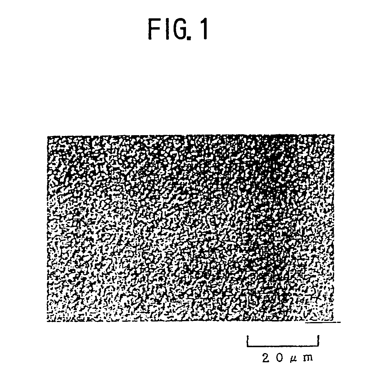
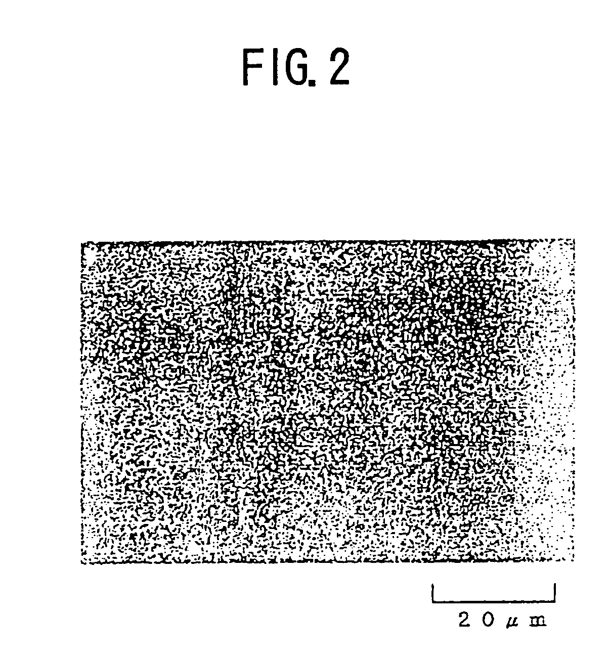
[0083]FIGS. 1 and 2 represent the surface of an AlGaInNP layer and a GaInNP layer formed on a GaAs substrate as the active layer of the light-emitting semiconductor device by an MOCVD process.

[0084]Referring to FIGS. 1 and 2, it should be noted that each of the AlGaInNP layer and the GaInNP layer was formed with a thickness of about 1 μm, and the deposition of the active layer was made on a crystal surface of the GaAs substrate inclined in the direction from the (100) surface by an angle of 15°. The deposition was made by using TMG (tetramethyl gallium), TMA (tetramethyl aluminum), TMI (tetramethyl indium) and PH3 as res...

second embodiment

[0088]FIG. 3 shows the construction of a semiconductor layered structure 10 according to a second embodiment of the present invention.

[0089]Referring to FIG. 3, the semiconductor layered structure 10 includes an SOW (single quantum well) structure formed on a GaAs substrate 11 by an MOCVD process, wherein the SQW structure is formed on a buffer layer (not shown) of undoped GaAs formed on the GaAs substrate 11 epitaxially with a thickness of about 0.2 μm. The SQW structure, in turn, includes a barrier layer 13 of undoped AlGaInP having a composition of (Al0.5Ga0.5)0.49In0.51P, wherein the barrier layer 13 is formed on the buffer layer epitaxially with a thickness of about 0.2 μm. The barrier layer 13, in turn, is covered by an intermediate layer 14 of undoped GaInP having a composition of Ga0.65In0.35P and formed epitaxially on the barrier layer 13 with a thickness of about 1.2 nm, and an active layer 15 of undoped GaInNP having a composition of Ga0.65In035N0.008P0.992 is formed epit...

third embodiment

[0097]FIG. 5 shows the construction of a stripe laser diode 500 according to a third embodiment of the present invention based on the layered structure 10 of FIG. 3.

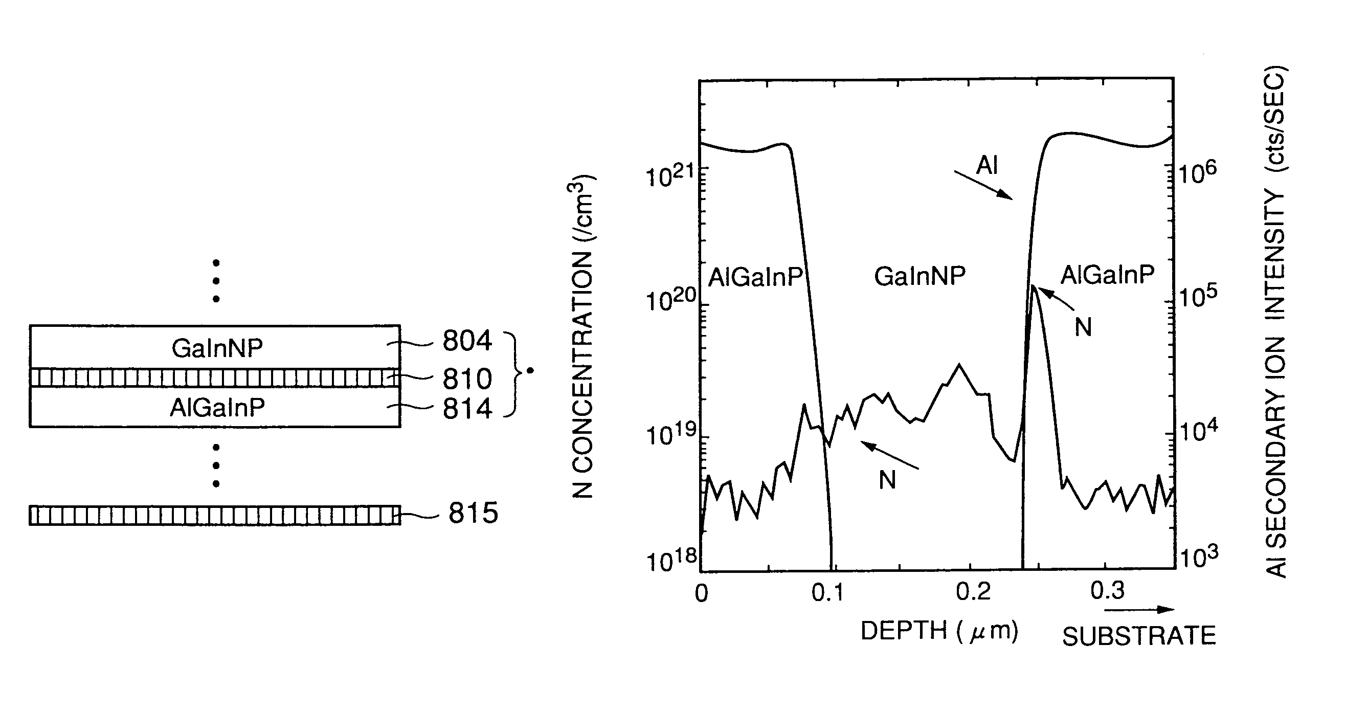
[0098]Referring to FIG. 5, the laser diode 500 is constructed on a substrate 501 of n-type GaAs having a principal surface inclined in the direction from the (100) surface of GaAs by an angle of about 15° and includes a buffer layer 502 of n-type GaAs formed epitaxially on the foregoing principal surface of the substrate 501, wherein the buffer layer 502 carries thereon a lower cladding layer 503 of n-type AlGaInP formed epitaxially with a composition of (Al0.7Ga0.3)0.51In0.49P, while the lower cladding layer 503 carries thereon an active layer 504 of undoped GaInNP formed also epitaxially with a composition of Ga0.51In0.49N0.01P0.99, wherein an intermediate layer 510 of GaP is interposed between the lower cladding layer 503 and the active layer 504. The intermediate layer 510 thus formed has a thickness of about 2 mole...


PUM

PropertyMeasurementUnit
temperatureaaaaaaaaaa
wavelength bandaaaaaaaaaa
optical wavelength bandaaaaaaaaaa

Abstract

An optical semiconductor device operable in a 0.6 μm band includes an active layer of GaInNP sandwiched by a pair of GaInP layer with a thickness of about 2 molecular layers or less.

Description

[0001]This application is a divisional application of U.S. patent application Ser. No. 09 / 289,955, filed Apr. 13, 1999, the entirety of which is incorporated herein by reference. Now U.S. Pat. No. 6,563,851.BACKGROUND OF THE INVENTION[0002]The present invention generally relates to optical semiconductor devices and more particularly to an optical semiconductor device including a laser diode operable in a 0.6 μm wavelength band.[0003]The optical wavelength band of 0.6 μm is used extensively in storage devices such as an optical disk drive or a magneto-optical disk drive for optical writing or reading of information. Further, the optical wavelength band of 0.6 μm is important in optical telecommunication that is conducted by using plastic optical fibers.[0004]Thus, intensive investigations are being made in relation to a laser diode of an AlGaInP system that produces an output optical beam with the optical wavelength band of 0.6 μm. The laser diode using the AlGaInP system is also imp...

Claims


Application Information

Patent Timeline
Patent Type & Authority Patents(United States)
IPC IPC(8): H01L21/00C30B25/00H01S5/183H01S5/20H01S5/323H01S5/34H01S5/343
CPCB82Y20/00H01S5/34H01S5/34326H01S5/18308H01S5/18341H01S5/18369H01S5/2063H01S5/32358H01S5/3403H01S5/3436
Inventor SATO, SHUNICHI
Owner RICOH KK
Why Eureka
Try Eureka