
High yield method for preparing silicon nanocrystal with chemically accessible surfaces

a technology of silicon nanocrystals and high yield, applied in the direction of crystal growth process, polycrystalline material growth, silicon compounds, etc., can solve the problems of nanocrystalline silicon utilization, lack of high yield synthetic method, and surface oxide contamination

Inactive Publication Date: 2007-05-08
EVERGREEN SOLAR
View PDF24 Cites 4 Cited by
  • Summary
  • Abstract
  • Description
  • Claims
  • Application Information

AI Technical Summary

Benefits of technology

This method enables the production of high-yield, well-defined silicon nanocrystals with controlled size and shape, free from surface contamination, and stability under ambient conditions, facilitating their use in various technological and biomedical applications.

Problems solved by technology

The largest barrier to the utilization of nanocrystalline silicon is the lack of a high yield synthetic method that gives rise to good quality silicon nanocrystals.
In addition, these techniques often give rise to surface oxide contamination.

Method used


Image

  • High yield method for preparing silicon nanocrystal with chemically accessible surfaces
  • High yield method for preparing silicon nanocrystal with chemically accessible surfaces
  • High yield method for preparing silicon nanocrystal with chemically accessible surfaces

Examples


example 1

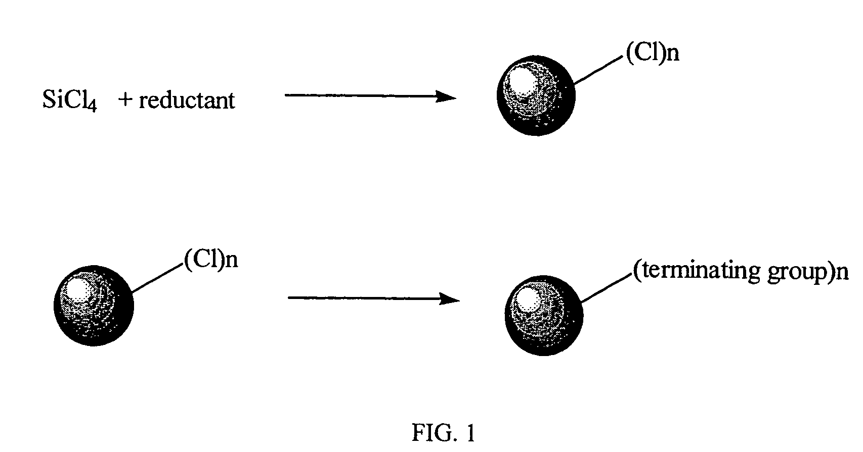
[0037]A tetrahydrofuran solution of sodium naphthalenide (0.9 g, 39 mmol Na and 3.23 g, 25 mmol of naphthalene in 30 cm3 tetrahydrofuran stirred for three hours) was added rapidly at room temperature via cannula to a 500 cm3 Schlenk flask containing 300 cm3 of 1,2-dimethoxyethane and 1.14 g, 6.7 mmol of SiCl4 with rapid stirring. On completion of the naphthalenide addition a large excess of n-butyllithium (10 cm3, 1.6M in hexane) was added immediately. The solvent was removed under vacuum from the resulting yellow brown suspension. The residue was extracted with hexane and washed with water to remove sodium and lithium salts. Evaporation of the hexane layer followed by heating under vacuum to remove residual naphthalene gave 0.7 g of a viscous yellow oil.

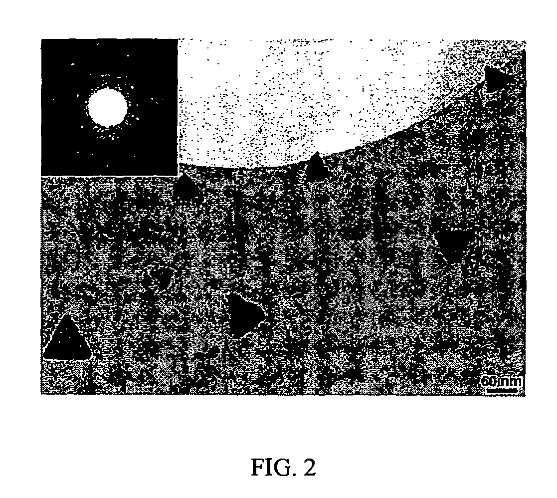
[0038]Transmission electron microscopy (TEM) shows the presence of crystalline silicon tetrahedra of approximately 60 nm in edge length. The bright-field TEM image of a number of the silicon nanocrystals on a holey carbon grid, alon...

example 2

[0040]Sodium naphthalenide, prepared from sodium (0.69 g) and nanphthalene (2.39 g) stirred in 70 cm3 of 1,2-dimethoxyethane overnight, was added rapidly via cannula to a stirred solution of 1.04 g of SiCl4 in 1,2-dimethoxyethane. The dark brown suspension obtained was stirred for a further 30 minutes then 5 cm3 of 1-octanol was added. A yellow solution with a white precipitate was observed immediately. The solvent and naphthalene were removed immediately with heating in a water bath. The resulting orange solid was extracted with hexane and washed three times with slightly acidic distilled water. The hexane layer was collected and pumped down to give a waxy orange hexane soluble solid. Solution 1H NMR was consistent with octanoxide groups on the surface of the nanocrystals. This was also supported by the IR spectrum in which a Si—OR stretch was observed at ˜1080 cm−1 and an alkyl C—H stretch at 3000 cm−1. The nanocrystals

[0041]Holey carbon grids for TEM were prepared by suspending t...

example 3

[0042]Magnesium powder (0.47 g) was suspended with sonication in 70 cm3 of dry 1,2-dimethoxyethane. To this was added 1.18 cm3 of SiCl4 and the resulting suspension sonicated overnight. To the red / brown solution and gray precipitate thus obtained was added 2 cm3 of 20% MgBuCl in tetrahydrofuran. The solvent and any other volatiles were removed under vacuum, the resulting colorless oil taken up in hexane, washed with slightly acidified water and again pumped down to a colorless oil. The oil contained small silicon nanoparticles by TEM (1H NMR and IR confirmed the existence of terminating butyl groups.


PUM

PropertyMeasurementUnit
size distributionaaaaaaaaaa

Abstract

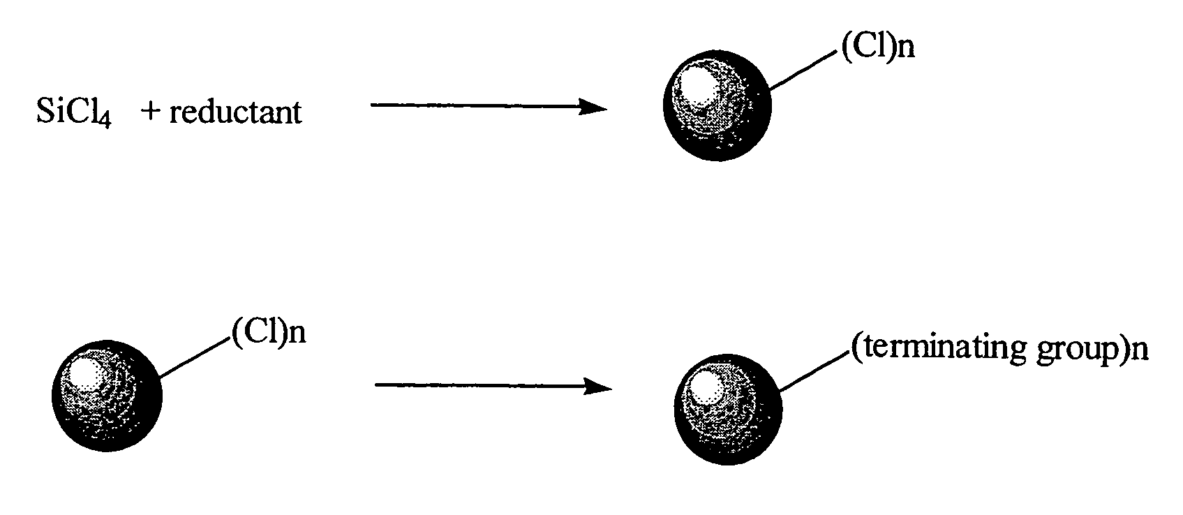
Silicon nanocrystals with chemically accessible surfaces are produced in solution in high yield. Silicon tetrahalide such as silicon tetrachloride (SiCl4) can be reduced in organic solvents, such as 1,2-dimethoxyethane(glyme), with soluble reducing agents, such as sodium naphthalenide, to give halide-terminated (e.g., chloride-terminated) silicon nanocrystals, which can then be easily functionalized with alkyl lithium, Grignard or other reagents to give easily processed silicon nanocrystals with an air and moisture stable surface. The synthesis can be used to prepare alkyl-terminated nanocrystals at ambient temperature and pressure in high yield. The two-step process allows a wide range of surface functionality.

Description

RELATED APPLICATIONS[0001]This application is a continuation of application Ser. No. 10 / 247,757, filed on Sep. 19, 2002 now U.S. Pat. No. 6,855,204, which claims the benefit of the filing date of U.S. Provisional Patent Application Ser. No. 60 / 323,285, filed on Sep. 19, 2001, entitled “HIGH YIELD METHOD FOR PREPARING SILICON NANOCRYSTALS WITH CHEMICALLY ACCESSIBLE SURFACES” by Kauzlarich et al., the entire disclosure of which are both incorporated herein by reference.GOVERNMENT RIGHTS[0002]The subject matter described herein was supported in part by NIST Advanced Technology Program, Contract No. 70 NANBOH3028. The U.S. Government has certain rights in this invention.TECHNICAL FIELD[0003]The invention generally relates to silicon nanocrystals. More particularly, the invention relates to silicon nanocrystals having chemically accessible surfaces and methods of their preparation.BACKGROUND OF THE INVENTION[0004]There has been relatively little research into the synthesis of silicon nan...

Claims


Application Information

Patent Timeline
Patent Type & Authority Patents(United States)
IPC IPC(8): H01L21/20C01B33/023C01B33/033C30B7/00C30B29/66
CPCB82Y30/00C01B33/033C30B7/00C30B29/605C30B29/06Y10S977/773Y10S977/896Y10S977/775Y10S977/776Y10S977/813Y10S977/814
Inventor KAUZLARICH, SUSAN M.BALDWIN, RICHARD K.
Owner EVERGREEN SOLAR
Learn More