Method for manufacturing a semiconductor device where the scanning direction changes between regions during crystallization and process

a semiconductor device and crystallization process technology, applied in the direction of manufacturing tools, solid-state devices, laser beam welding apparatus, etc., can solve the problems of long irradiation time, inability to perform laser processing uniformly, and inability to achieve uniform crystallinity, uniform electric characteristic, and uniform crystallinity. uniform

Active Publication Date: 2007-05-22
SEMICON ENERGY LAB CO LTD
View PDF28 Cites 20 Cited by
  • Summary
  • Abstract
  • Description
  • Claims
  • Application Information

AI Technical Summary

Benefits of technology

[0030]Moreover, when a semiconductor film is used as the irradiated object, it is possible to provide the poly-crystalline TFT having uniform crystallinity and uniform electric characteristic. With such a poly-crystalline TFT equipped, advantageous effects such as uniformity of the display and enhancement of the performance can be expected in a liquid crystal display device, a display device such as a light-emitting device having a self light-emitting element and an integrated circuit having a CPU and a memory.
[0031]It is noted that after the irradiated object and the beam relatively move to process one line, they move on to the next line. Such a relative movement is repeated to process a large area. Therefore, the scanning speed of the laser beam and the scanning speed of the irradiated object are set so as to synchronize each other. In other words, first scanning means for changing the traveling direction (scanning direction) of the laser beam and second scanning means for scanning the irradiated object relative to the first scanning means are controlled so as to synchronize each other.
[0032]In addition, it is preferable to arrange an fθ lens between the irradiated object and the scanning means in order to make the spot of the laser beam have a constant shape. It is more preferable to employ a telecentric fθ lens that can make an incidence angle constant. Although there is a limit for enlarging the size of such an fθ lens, the fθ lens can process a wide range of region by moving the irradiated object in XY directions.
[0033]In the case of irradiating in the laser beam uniformly, that is, scanning the laser beam at constant speed, the element-forming region in the irradiated object can be irradiated and thus uniform irradiation method of the laser beam can be provided according to the present invention.
[0034]Moreover, when a semiconductor film is used as the irradiated object, it is possible to provide the poly-crystalline TFT having uniform crystallinity and uniform electric characteristic. With such a poly-crystalline TFT equipped, advantageous effects such as uniformity of the display and enhancement of the performance can be expected in a liquid crystal display device, a display device such as a light-emitting device having a self light-emitting element and an integrated circuit having a CPU and a memory.
[0035]In the present invention, the beam can be irradiated uniformly by irradiating the beam to the outside of the display device, which is the outside of the element-forming region, when the CW beam is employed and when the scanning speed of the beam is not uniform. In other words, the laser annealing with the laser used as the light source can be performed uniformly. As a result, mass productivity is enhanced and the display device can be manufactured at lower cost.EFFECT OF THE INVENTION

Problems solved by technology

The region where the scanning of the laser light stops makes it difficult to perform the laser processing uniformly.
Furthermore, the speed of the laser light scanned by the scanning means such as the galvanometer mirror or the polygon mirror was not constant in the center portion and in the end portion of the scanning width.
In such regions where the scanning speed decelerates, accelerates, and becomes zero, the irradiation time becomes longer so that the object is irradiated with excessive energy.
As a result, when the amorphous semiconductor film is used as the irradiated object, there is a risk that the amorphous semiconductor film is peeled or the like.
As a result, there is also a risk, as well as the galvanometer mirror, that the amorphous semiconductor film is peeled or the like.
It is concerned that when the semiconductor film is peeled, the peeled film is spattered to the normal film, which results in the roughness of the normal film.

Method used


Image

  • Method for manufacturing a semiconductor device where the scanning direction changes between regions during crystallization and process
  • Method for manufacturing a semiconductor device where the scanning direction changes between regions during crystallization and process
  • Method for manufacturing a semiconductor device where the scanning direction changes between regions during crystallization and process

Examples


embodiment mode 1

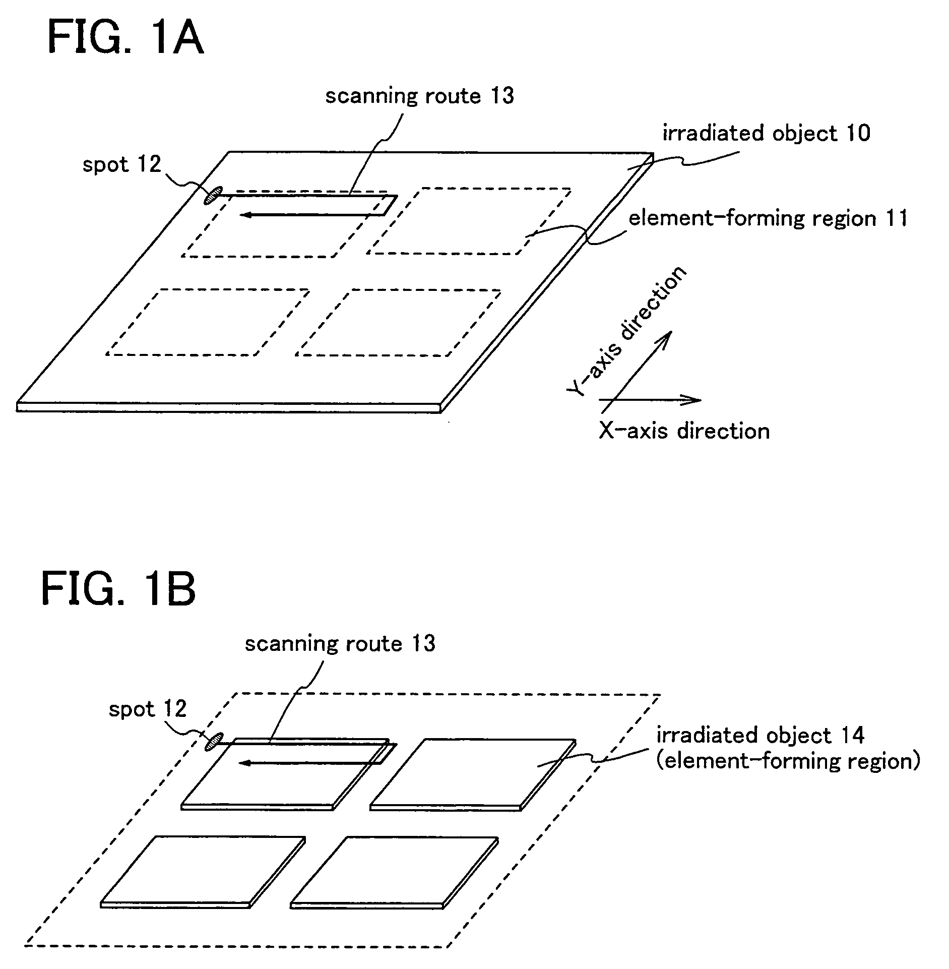
[0044]The present embodiment mode explains the case in which the laser processing is performed by employing the laser as the light source to the irradiated object in which four element-forming regions are formed.

[0045]In a perspective diagram shown in FIG. 1(A), four of an element-forming regions 11 are provided in an irradiated object 10. And relative movements of the laser beam and the irradiated object move a spot 12 along a scanning route 13. The scanning route 13 is in XY directions where a major axis direction (X-axis direction in FIG. 1(A)) and a minor axis direction (Y-axis direction in FIG. 1(A)) are combined. On this occasion, for example, the first scanning means (for example, the galvanometer mirror or the polygon mirror) moves the spot in the major axis direction and the second scanning means (for example, an XY stage) moves the irradiated object in the minor axis direction. As thus described, the laser processing can be performed to the whole irradiated object having a...

embodiment mode 2

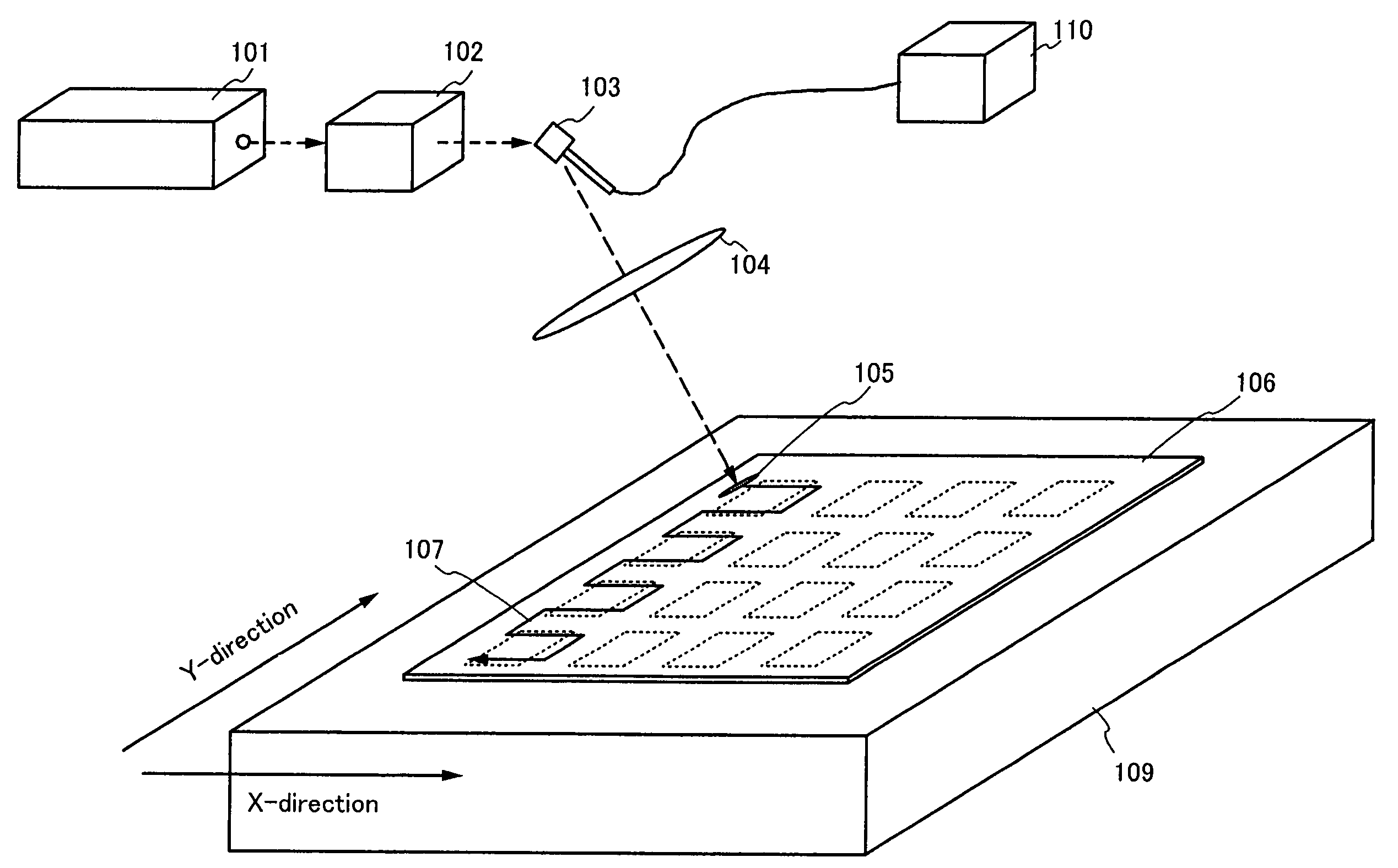
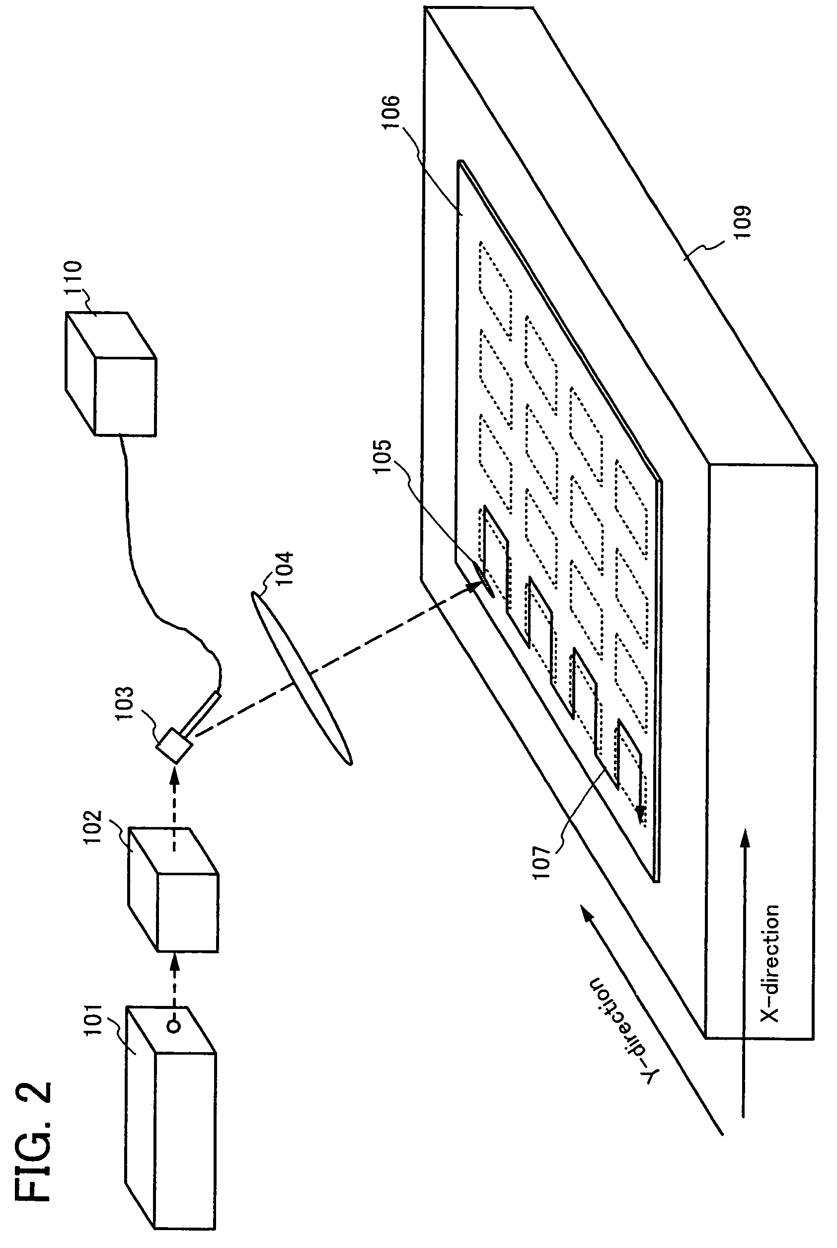
[0060]The present embodiment mode explains a beam irradiation apparatus, which means a laser irradiation apparatus, and a beam irradiation method, which means a laser irradiation method using a CW laser as one mode of the beam, with reference to FIG. 2. In addition, the present embodiment mode explains one example in which a semiconductor film is used as the irradiated object and a galvanometer mirror is used as the first scanning means.

[0061]Initially, the CW laser emitted from a laser oscillator 101 is extended long through an optical system 102 and shaped into linear. Specifically, the laser beam can be shaped into linear by transmitting through a cylindrical lens and a convex lens in the optical system 102.

[0062]After that, the laser beam shaped into linear (also referred to as a linear beam) is incident into a semiconductor film 106 through a galvanometer mirror 103 and an fθ lens 104. On this occasion, the linear beam is adjusted so as to form a spot 105 of the laser (hereinaf...

embodiment mode 3

[0073]This embodiment mode explains the case to enhance productivity of the integrated circuit having the thin film transistor by performing the laser processing to the semiconductor film formed over the substrate with a laser irradiation apparatus including a plurality of laser oscillators.

[0074]FIG. 3 shows an example to employ three CW laser oscillators 201, three telecentric fθ lenses 204, three galvanometer mirrors 203, and three pairs of slits 207 to perform the laser-sized processing, that is, the laser annealing to a semiconductor film 205 formed over a large substrate having a size of 1500 mm×1800 mm. It is noted that FIG. 3(A) is a top view and FIG. 3(B) is a side view.

[0075]An oxide film (a silicon oxide film such as SiON or SiO2) is formed over a substrate as a base film and then a semiconductor film is formed thereon sequentially. The semiconductor film may be formed of the material mainly consisting of silicon by CVD, sputtering, or the like. In this embodiment mode, a...


PUM

PropertyMeasurementUnit
sizeaaaaaaaaaa
widthaaaaaaaaaa
angleaaaaaaaaaa

Abstract

The speed of the laser scanned by the scanning means such as a galvanometer mirror or a polygon mirror is not constant in the center portion and in the end portion of the scanning width. As a result, the object, for example an amorphous semiconductor film, is irradiated with the excessive energy and therefore there is a risk that the amorphous semiconductor film is peeled. In the present invention, in the case where the laser spot of the energy beam output continuously on the irradiated object is scanned by moving it back and forth with the use of the scanning means or the like, the beam is irradiated to the outside of the element-forming region when the scanning speed of the spot is not the predetermined value, for example when the speed is not constant, and accelerates, decelerates, or is zero, for example in the positions where the scanning direction changes, or where the scanning starts or ends.

Description

BACKGROUND OF THE INVENTION[0001]1. Field of the Invention[0002]The present invention relates to a beam irradiation apparatus and a beam irradiation method. Moreover, the present invention relates to a method for manufacturing a thin film transistor using the apparatus and the method.[0003]2. Description of Related Art[0004]A research has been conducted concerning a thin film transistor having a channel-forming region in a poly-crystalline semiconductor film (hereinafter this thin film transistor is referred to as poly-crystalline TFT) as a semiconductor element in a display device, an integrated circuit, or the like. With the development of the display device and the integrated circuit, further enhancement of the characteristic of the poly-crystalline TFT has been expected.[0005]Consequently, in order to enhance the characteristic of the poly-crystalline TFT, crystallization of the semiconductor film by a continuous wave laser irradiation apparatus has been examined. For example, t...

Claims


Application Information

Patent Timeline
Patent Type & Authority Patents(United States)
IPC IPC(8): H01L21/00B23K26/08H01L21/20H01L21/77H01L21/84
CPCB23K26/0807H01L27/1285H01L21/2026B23K26/0815B23K26/0821B23K26/082H01L21/02592H01L21/02683H01L21/02488H01L21/02422H01L21/0242H01L21/02425H01L21/02686H01L21/02678H01L21/02532H01L21/02595H01L21/02381H01L21/02691
Inventor YAMAZAKI, SHUNPEITANAKA, KOICHIROMIYAIRI, HIDEKAZU
Owner SEMICON ENERGY LAB CO LTD
Why Eureka
Try Eureka