Methods to deposit metal alloy barrier layers

a metal alloy and layer technology, applied in the direction of liquid/solution decomposition chemical coating, semiconductor/solid-state device details, coatings, etc., can solve the problems of voids within the connection between the die, failure of the device, and excessive hea

Inactive Publication Date: 2007-05-29
INTEL CORP +1
View PDF31 Cites 18 Cited by
  • Summary
  • Abstract
  • Description
  • Claims
  • Application Information

AI Technical Summary

Problems solved by technology

Copper presents different engineering challenges during different stages of the semiconductor fabrication process.
One such challenge is the formation of copper and tin intermetallic compounds on the interface between copper bumps on a die and the tin-based solder used to electrically connect that die to a substrate package, such as a ball grid array (BGA) or pin grid array (PGA), in a flip-chip process.
The diffusion of the copper and of the tin creates voids within the connection between the die and the package carrier.
The voids cause shorts, excessive heat, and eventually failure of the device.
But, these barrier layers do not effectively block the diffusion of copper and tin.
These refractory metal based barrier layers also became very brittle under the stresses placed on the package during fabrication and during the use of the device.
Another challenge of copper is the electromigration of copper from the interconnect lines and the vias of an integrated circuit into the surrounding dielectric material, particularly when the surrounding dielectric material is a porous low-k dielectric material.
However, these materials may be oxidized, removed, or corroded during the etching or cleaning of vias or trenches.
Also, copper may migrate through the cobalt containing materials into the surrounding dielectrics causing shorts, or oxygen may migrate into the copper through the cobalt based material causing oxidation of the copper interconnects.

Method used


Image

  • Methods to deposit metal alloy barrier layers
  • Methods to deposit metal alloy barrier layers
  • Methods to deposit metal alloy barrier layers

Examples


Embodiment Construction

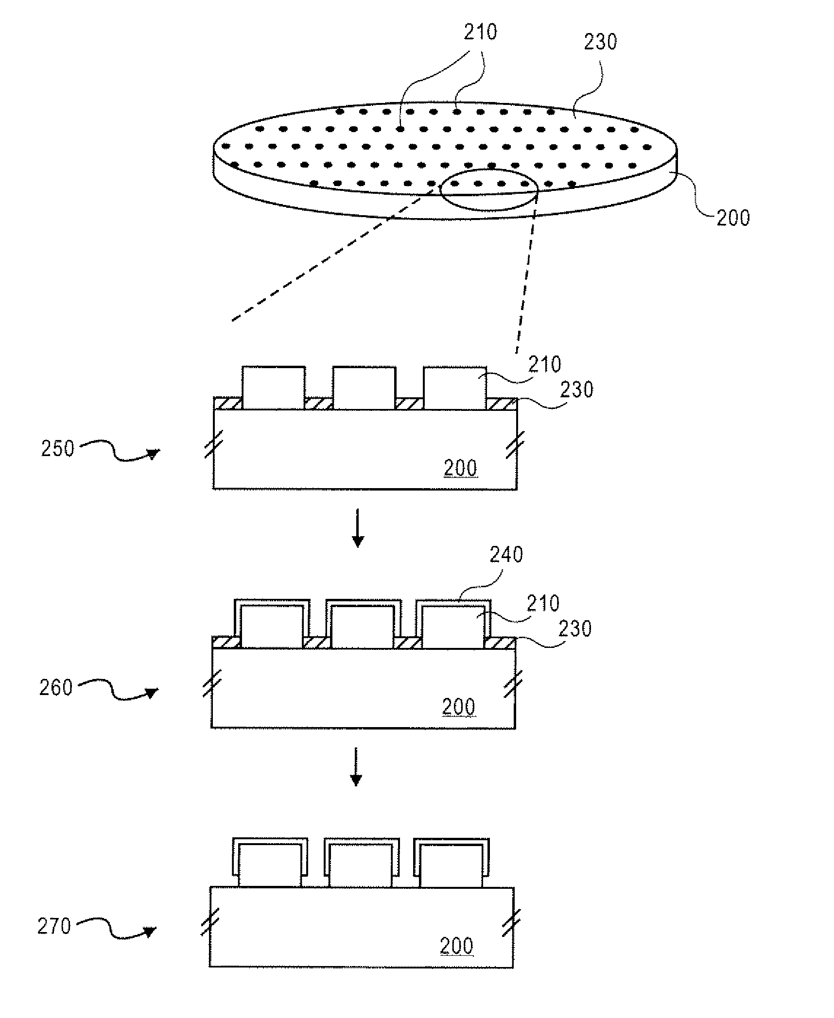
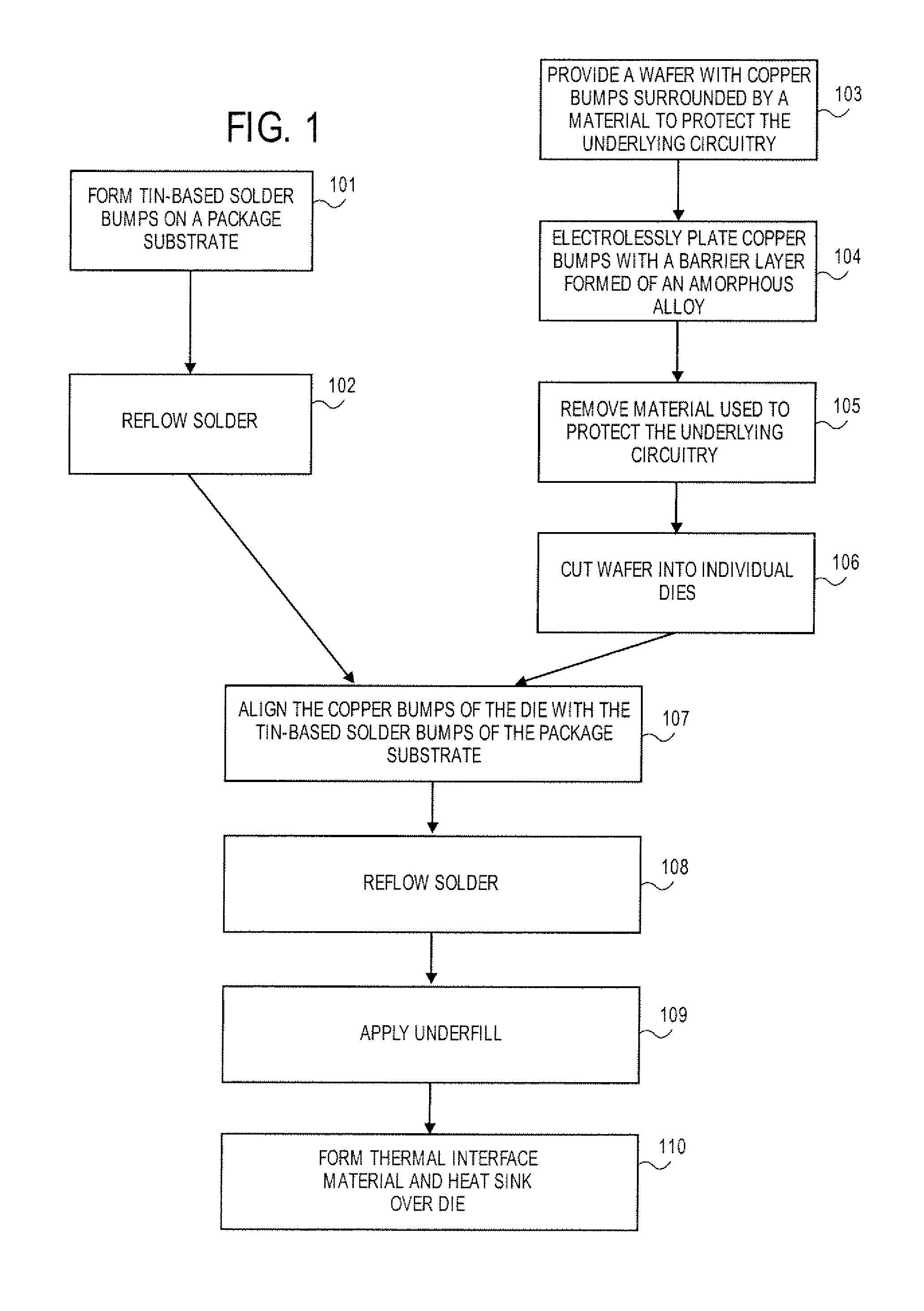
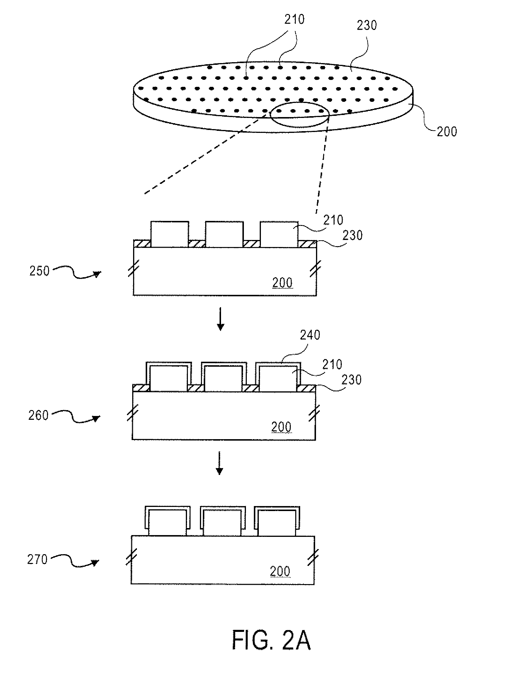
[0010]Described herein are methods of forming metal alloy group VIII-based diffusion barriers over copper. In the following description numerous specific details are set forth. One of ordinary skill in the art, however, will appreciate that these specific details are not necessary to practice embodiments of the invention. While certain exemplary embodiments of the invention are described and shown in the accompanying drawings, it is to be understood that such embodiments are merely illustrative and not restrictive of the current invention, and that this invention is not restricted to the specific constructions and arrangements shown and described because modifications may occur to those ordinarily skilled in the art. In other instances, well known semiconductor fabrication processes, techniques, materials, equipment, etc., have not been set forth in particular detail in order to not unnecessarily obscure embodiments of the present invention.

[0011]The diffusion of elements through ba...


PUM

PropertyMeasurementUnit
thicknessaaaaaaaaaa
temperatureaaaaaaaaaa

Abstract

Metal alloy barrier layers formed of a group VIII metal alloyed with boron (B) and / or phosphorous (P) and an at least one element from glyoxylic acid, such as carbon (C), hydrogen (H), or carbon and hydrogen (CH) formed by electoless plating are described. These barrier layers may be used as a barrier layer over copper bumps that are soldered to a tin-based solder in a die package. Such barrier layers may also be used as barrier layer liners within trenches in which copper interconnects or vias are formed and as capping layers over copper interconnects or vias to prevent the electromigration of copper.

Description

BACKGROUND OF THE INVENTION[0001]1. Field of the Invention[0002]The present invention relates to the field of semiconductor fabrication and processing and more particularly to the field of the electroless deposition of metal alloy barrier layers over copper.[0003]2. Discussion of Related Art[0004]Copper presents different engineering challenges during different stages of the semiconductor fabrication process. One such challenge is the formation of copper and tin intermetallic compounds on the interface between copper bumps on a die and the tin-based solder used to electrically connect that die to a substrate package, such as a ball grid array (BGA) or pin grid array (PGA), in a flip-chip process. The flip-chip process is a method to electrically connect the die to the package carrier. The package carrier, either a substrate or a leadframe, then provides the connection from the die to the exterior of the package. The interconnection between the die and the carrier in flip chip packag...

Claims


Application Information

Patent Timeline
Patent Type & Authority Patents(United States)
IPC IPC(8): H01L21/44
CPCC23C18/32C23C18/34C23C18/36H01L21/288H01L21/76843H01L21/76849H01L21/76852H01L21/76874H01L23/36H01L23/53238H01L24/11H01L24/13H01L21/563H01L2224/13099H01L2224/13147H01L2924/01005H01L2924/01011H01L2924/01015H01L2924/01027H01L2924/01029H01L2924/01046H01L2924/01073H01L2924/01075H01L2924/01077H01L2924/01078H01L2924/01327H01L2924/04953H01L2924/14H01L2924/15312H01L2924/16152H01L2924/01006H01L2924/01019H01L2924/01023H01L2924/01044H01L2924/01045H01L2924/01076H01L2924/014H01L2224/16225H01L2224/32225H01L2224/73204H01L2924/00H01L2924/00013H01L2224/29099H01L2924/00014H01L2924/00011H01L2224/0401
Inventor ZHONG, TINGHUA, FAYDUBIN, VALERY M.
Owner INTEL CORP
Why Eureka
Try Eureka