

Method for achieving chemical nickel plating by activating surface of PCB
A technology of electroless nickel plating and electroless nickel plating solution, which is applied in liquid chemical plating, metal material coating process, coating and other directions, can solve the problems of high price, easy decomposition, poor stability of plating solution, etc., and reduce production costs. , The effect of fast activation speed and high bonding strength
- Summary
- Abstract
- Description
- Claims
- Application Information
AI Technical Summary
Problems solved by technology
Method used
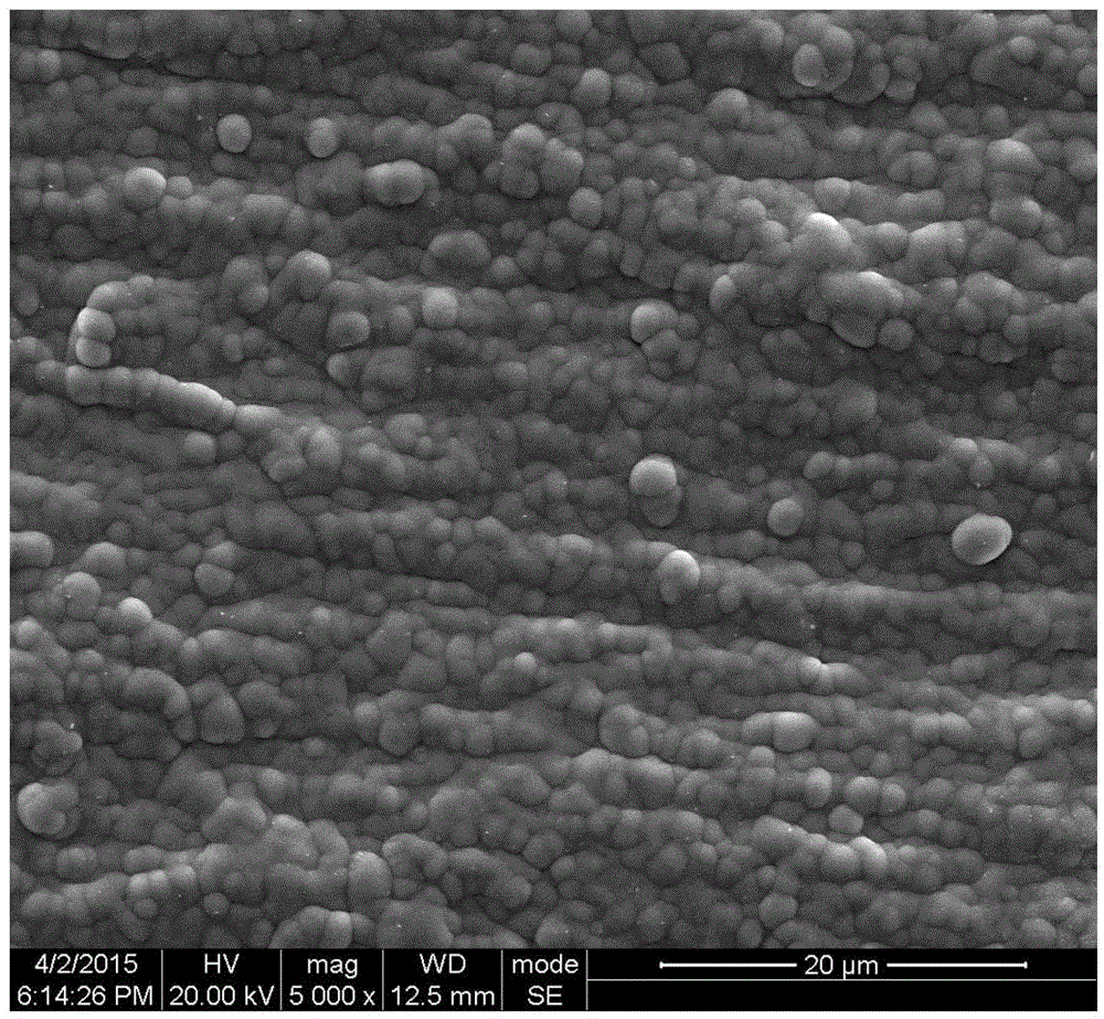
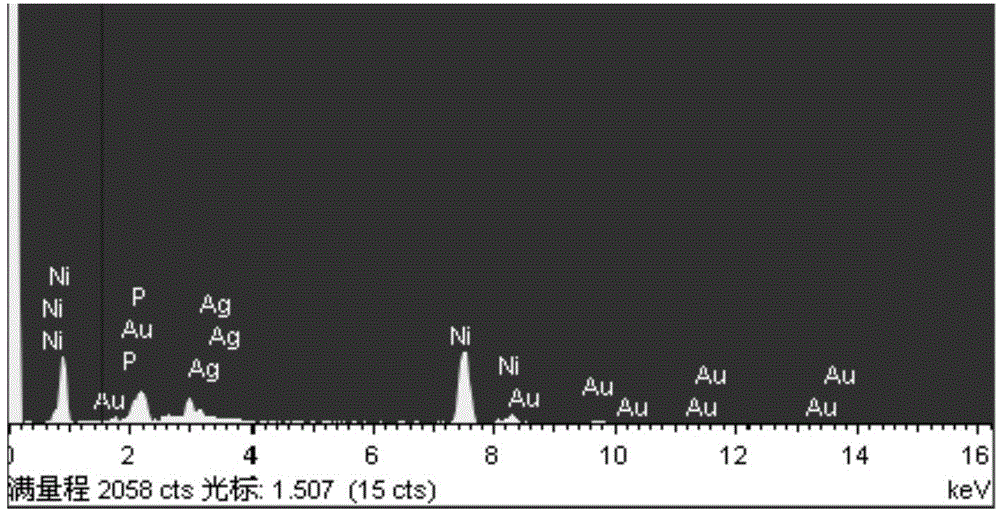
Image

Examples
Embodiment 1
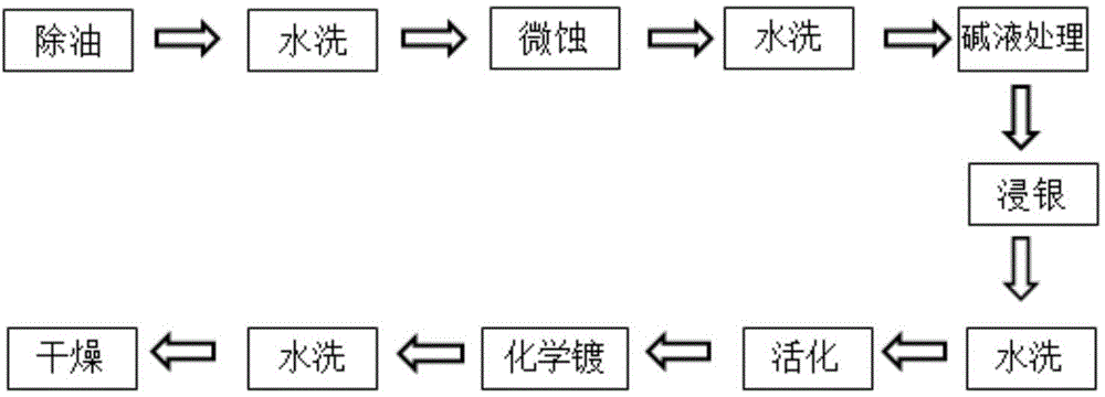
[0032] A method for activating the surface of a PCB circuit to realize electroless nickel plating, comprising the following steps:
[0033] Step 1. Preparation of silver immersion solution: add 0.2g silver nitrate, 0.2g silver acetate, 0.2g silver sulfate, 0.2g silver fluoride, 0.2g silver perchlorate and 0.1g EDTA into 1L deionized water, stir until completely dissolved , to obtain silver immersion solution;
[0034] Step 2. Preparation of activation solution: Add 20g of sodium hydroxide and 10g of formaldehyde into 1L of deionized water, stir until completely dissolved to obtain an activation solution;
[0035] Step 3. Pretreatment of PCB board: a. Add 25mL Rohm and Haas (LP200) and 5mL concentrated sulfuric acid to 1L deionized water in turn, mix well to obtain degreasing liquid; b. Add 10mL concentrated sulfuric acid and 20g sodium persulfate Add 1L of deionized water and mix evenly to obtain a microetching solution; c. Immerse the PCB board printed with copper circuits i...
Embodiment 2
[0040] A method for activating the surface of a PCB circuit to realize electroless nickel plating, comprising the following steps:
[0041] Step 1. Preparation of the silver immersion solution: add 1 g of silver nitrate to 1 L of deionized water, stir until completely dissolved, and obtain the silver immersion solution;
[0042] Step 2. Preparation of activation solution: Add 20g of sodium hydroxide and 10g of formaldehyde into 1L of deionized water, stir until completely dissolved to obtain an activation solution;
[0043] Step 3. Pretreatment of PCB board: a. Add 25mL Rohm and Haas (LP200) and 5mL concentrated sulfuric acid to 1L deionized water in turn, mix well to obtain degreasing liquid; b. Add 10mL concentrated sulfuric acid and 20g sodium persulfate Add 1L of deionized water and mix evenly to obtain a microetching solution; c. Immerse the PCB board printed with copper circuits in a degreasing solution at a temperature of 50°C for 30 minutes, then rinse the PCB board wi...
Embodiment 3
[0047] A method for activating the surface of a PCB circuit to realize electroless nickel plating, comprising the following steps:
[0048] Step 1. Preparation of the silver immersion solution: add 10g of silver nitrate to 1L of deionized water, stir until completely dissolved, and obtain the silver immersion solution;
[0049] Step 2. Preparation of activation solution: Add 30g of sodium hydroxide and 10g of formaldehyde into 1L of deionized water, stir until completely dissolved to obtain an activation solution;
[0050] Step 3. Pretreatment of PCB board: a. Add 25mL Rohm and Haas (LP200) and 5mL concentrated sulfuric acid to 1L deionized water in turn, mix well to obtain degreasing liquid; b. Add 10mL concentrated sulfuric acid and 20g sodium persulfate Add 1L of deionized water and mix evenly to obtain a microetching solution; c. Immerse the PCB board printed with copper circuits in a degreasing solution at a temperature of 50°C for 30 minutes, then rinse the PCB board wit...
PUM
| Property | Measurement | Unit |
|---|---|---|
| diameter | aaaaa | aaaaa |
Abstract
Description
Claims
Application Information