Fabrication of strained heterojunction structures

a heterojunction structure and semiconductor technology, applied in the field of semiconductor processing, can solve the problems of difficult to have adjacent devices in different strain states, rough growth front, and high-quality strained silicon, and achieve the effects of improving carrier mobility, improving characteristics, and improving speed

US7229901B2Active Publication Date: 2007-06-12WISCONSIN ALUMNI RES FOUND
28 Cites 54 Cited by

Patent Information

Authority / Receiving Office
US · United States
Patent Type
Patents(United States)
Current Assignee / Owner
Publication Date
2007-06-12

Smart Images

  • Figure 1
    Figure 1
  • Figure 2
    Figure 2
  • Figure 3
    Figure 3
Patent Text Reader

Abstract

Growth of multilayer films is carried out in a manner which allows close control of the strain in the grown layers and complete release of the grown films to allow mounting of the released multilayer structures on selected substrates. A layer of material, such as silicon-germanium, is grown onto a template layer, such as silicon, of a substrate having a sacrificial layer on which the template layer is formed. The grown layer has a lattice mismatch with the template layer so that it is strained as deposited. A top layer of crystalline material, such as silicon, is grown on the alloy layer to form a multilayer structure with the grown layer and the template layer. The sacrificial layer is preferentially etched away to release the multilayer structure from the sacrificial layer, relaxing the grown layer and straining the crystalline layers interfaced with it.
Need to check novelty before this filing date? Find Prior Art

Description

REFERENCE TO GOVERNMENT RIGHTS

[0001] This invention was made with United States government support awarded by the following agency: NSF 0079983. The United States government has certain rights in this invention.FIELD OF THE INVENTION

[0002] This invention pertains generally to the field of semiconductor processing and particularly to the formation of strained heterojunction semiconductor structures.BACKGROUND OF THE INVENTION

[0003] Controlling the strain and the number and type of defects in heteroepitaxial semiconductor structures is crucial for obtaining high-quality semiconductor materials with the desired properties for forming high-performance devices. In the silicon / silicon-germanium hetero-system, appropriate control of the strain in the semiconductor layers provides control over band offsets and carrier mobility. Typically, it is desirable to be able to obtain a strain-relaxed SiGe virtual substrate on which a thin strained Si film is formed. The main obstacle to obtaining high-...

Examples

Embodiment Construction

[0030]The present invention provides a new approach for controlling strain in heterostructures. For purposes of exemplifying the invention, the following describes the production of silicon / silicon-germanium heterostructures which are formed on silicon-on-insulator (SOI) substrates and then released, but the invention may be implemented in any semiconductor system or other material system requiring strain control as discussed herein.

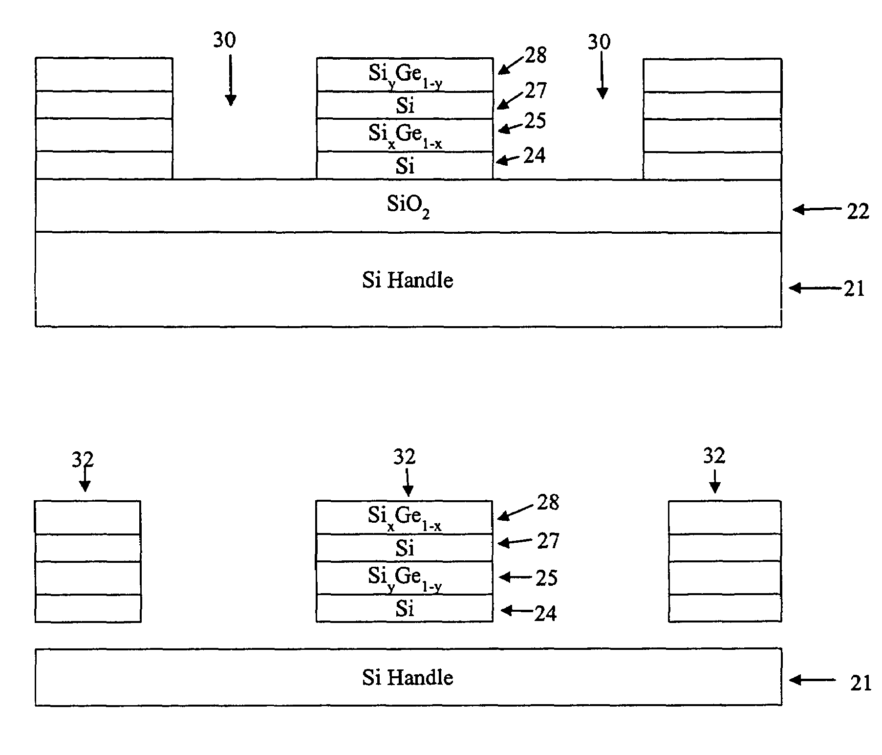
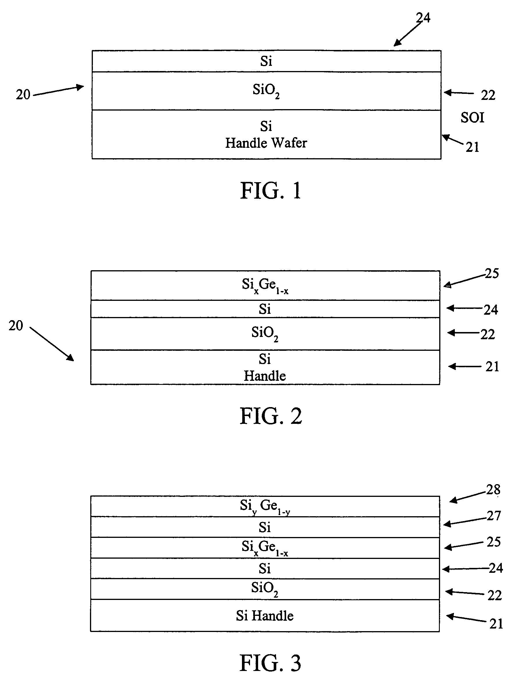
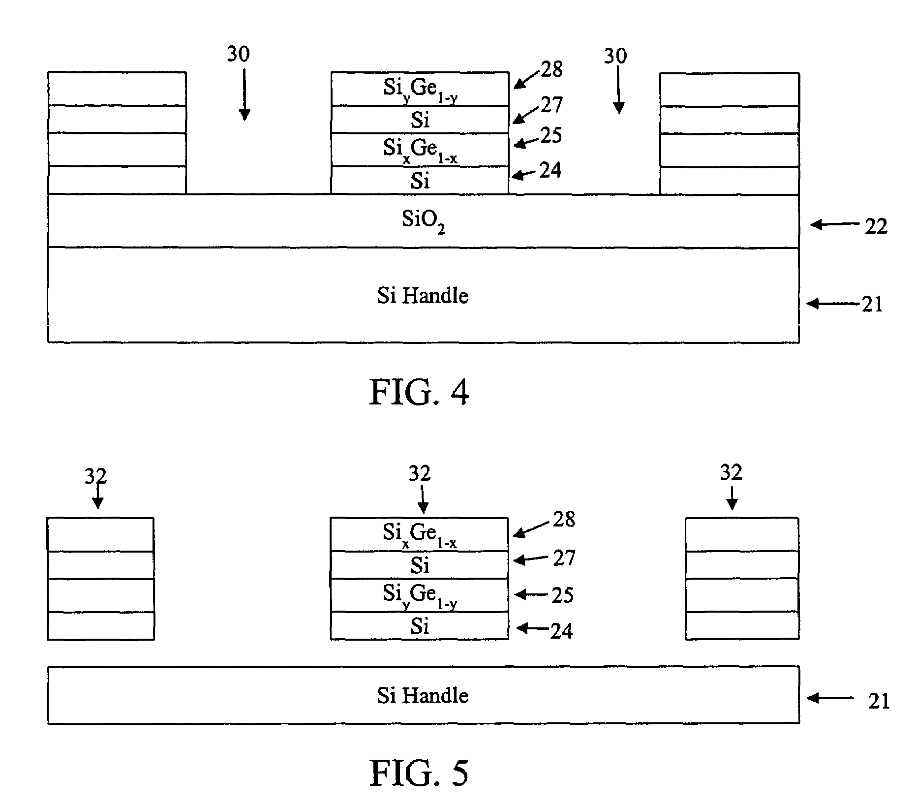
[0031]An initial SOI wafer is shown generally in cross-section at 20 in FIG. 1 and includes a crystalline silicon handle wafer 21, an insulating (sacrificial) layer 22 of SiO2, and a template layer 24 of crystalline silicon that is typically 10 to 100 nm thick. As shown in FIG. 2, an initial layer 25 of SiGe is grown epitaxially on the silicon template layer 24 by any suitable process, such as molecular beam epitaxy (MBE), chemical vapor deposition (CVD), sputter deposition, etc., with the SiGe layer 25 in a state of internal compressive strain as grown ...