Nonvolatile semiconductor memory device with tapered sidewall gate and method of manufacturing the same

a semiconductor memory and sidewall gate technology, applied in semiconductor devices, electrical devices, transistors, etc., can solve the problems of short circuit, insufficient isolation distance from the high-concentration diffusion layer, and increase the thickness of the gate insulator, so as to improve the charge storing characteristic, improve the size, and increase the current

Active Publication Date: 2007-06-26
RENESAS ELECTRONICS CORP
View PDF6 Cites 71 Cited by
  • Summary
  • Abstract
  • Description
  • Claims
  • Application Information

AI Technical Summary

Benefits of technology

[0008]As for the charge storing characteristic, a silicon oxide film 11, a silicon nitride film 12, and a silicon oxide film 13 (defined as an “ONO film” hereinafter) to be an insulator of a self-aligned gate electrode 10 has an L-shaped corner portion 14 when viewed from a section vertical to the word line, as shown in FIG. 2. Electrons are mainly injected to the silicon nitride film near the L-shaped corner by a write operation using a source side injection method. The silicon oxide film 11 to be a lower layer of the ONO film (defined as a “bottom oxide film”) is usually formed by the thermal oxidation process, while the silicon nitride film 12 to be an intermediate layer thereof and the silicon oxide film 13 to be an upper layer thereof (defined as a “top oxide film”) are formed by the chemical vapor deposition (CVD). Due to the nature of the CVD, the thickness of the silicon nitride film 12 and the silicon oxide film 13 tends to be locally reduced at each corner portion. Usually, the thickness reduction at the corner portion is eminent in the silicon oxide film in comparison to the silicon nitride film. For example, in the CVD for depositing a silicon oxide film by the thermal decomposition of a usual source gas such as silane, the deposition thickness on the vertical pattern sidewall is less than 80% of that of the flat portion, and the thickness near the corner portion is further reduced. Since the thickness of the top oxide film for preventing the leakage of the charges in the silicon nitride film is reduced at the corner portion in which the charge density is high, the charge storing characteristic falls below the level actually expected from the deposited thickness. Although it is possible to improve the charge storing characteristic by increasing the deposition thickness of the top oxide film, the increase of the gate insulator thickness is not preferable because it causes the degradation of transistor characteristic such as the reduction of on current.
[0020]By combining the effects mentioned above, it is possible to achieve a MONOS type nonvolatile memory using the split gate cell structure which can achieve the high-speed operation and has a good charge storing characteristic. Therefore, it becomes possible to improve the performance of the embedded microcomputer fabricated along with a nonvolatile memory and to reduce the manufacturing cost thereof.

Problems solved by technology

However, it also has the problems as follows.
Although it is possible to improve the charge storing characteristic by increasing the deposition thickness of the top oxide film, the increase of the gate insulator thickness is not preferable because it causes the degradation of transistor characteristic such as the reduction of on current.
However, since the underlying layer of the outer sidewall 17 made of a silicon oxide film is a curved sidewall surface of the self-aligned electrode 10, the process margin in the anisotropic etching is small and thus it becomes difficult to appropriately perform the etching.
Alternatively, there easily arises the drawback of the fact that the isolation distance from the high-concentration diffusion layer becomes insufficient and short-circuited.
Furthermore, there is also the structural problem that the short circuit tends to occur between the silicides due to the short distance between the self-aligned electrode 10 and the select gate electrode 15.

Method used


Image

  • Nonvolatile semiconductor memory device with tapered sidewall gate and method of manufacturing the same
  • Nonvolatile semiconductor memory device with tapered sidewall gate and method of manufacturing the same
  • Nonvolatile semiconductor memory device with tapered sidewall gate and method of manufacturing the same

Examples


first embodiment

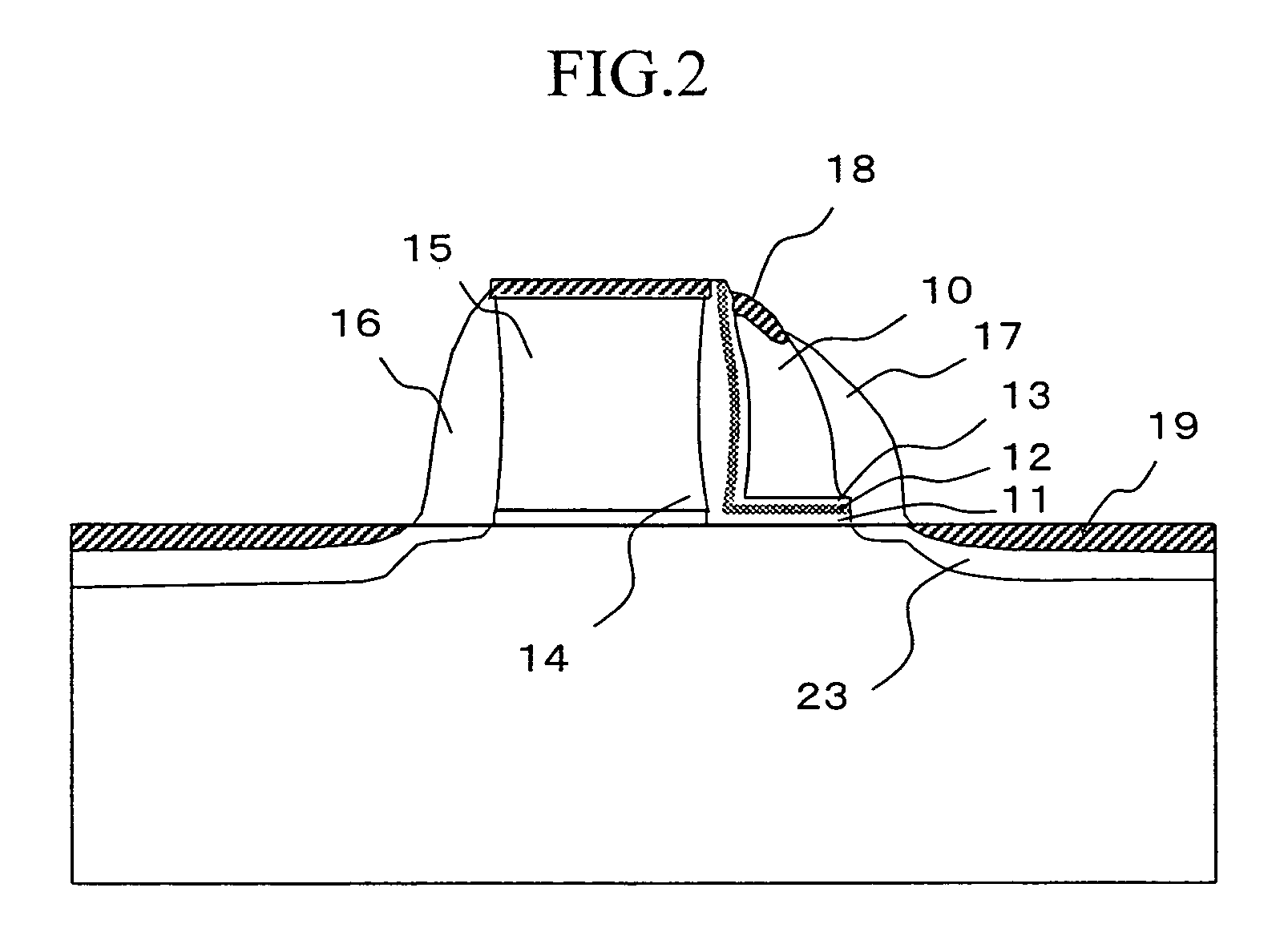
[0049]Hereinafter, a manufacturing process of a memory cell will be described. FIGS. 6 to 16 are enlarged sectional views vertical to the word line of the memory cell and correspond to a sectional view taken along the line (A)-(B) in FIG. 5. The general shallow trench isolation 33 which electrically isolates the devices is formed in the direction vertical to the word line, and a gate oxide film 40 is formed after the sacrificial oxidation of the surface of a silicon substrate for improving the interface quality (FIG. 6). Subsequently, polysilicon 41 with a thickness of 250 nm to be a material of the select gate electrode is deposited by the CVD, and a cap oxide film 42 with a thickness of 50 nm to be a mask in the subsequent process is deposited by the CVD. After coating a photoresist, the photoresist is patterned with a width of 180 nm by the photolithography process, and the cap oxide film 42 is removed by the dry etching with using the photoresist as a mask, and then the polysili...

second embodiment

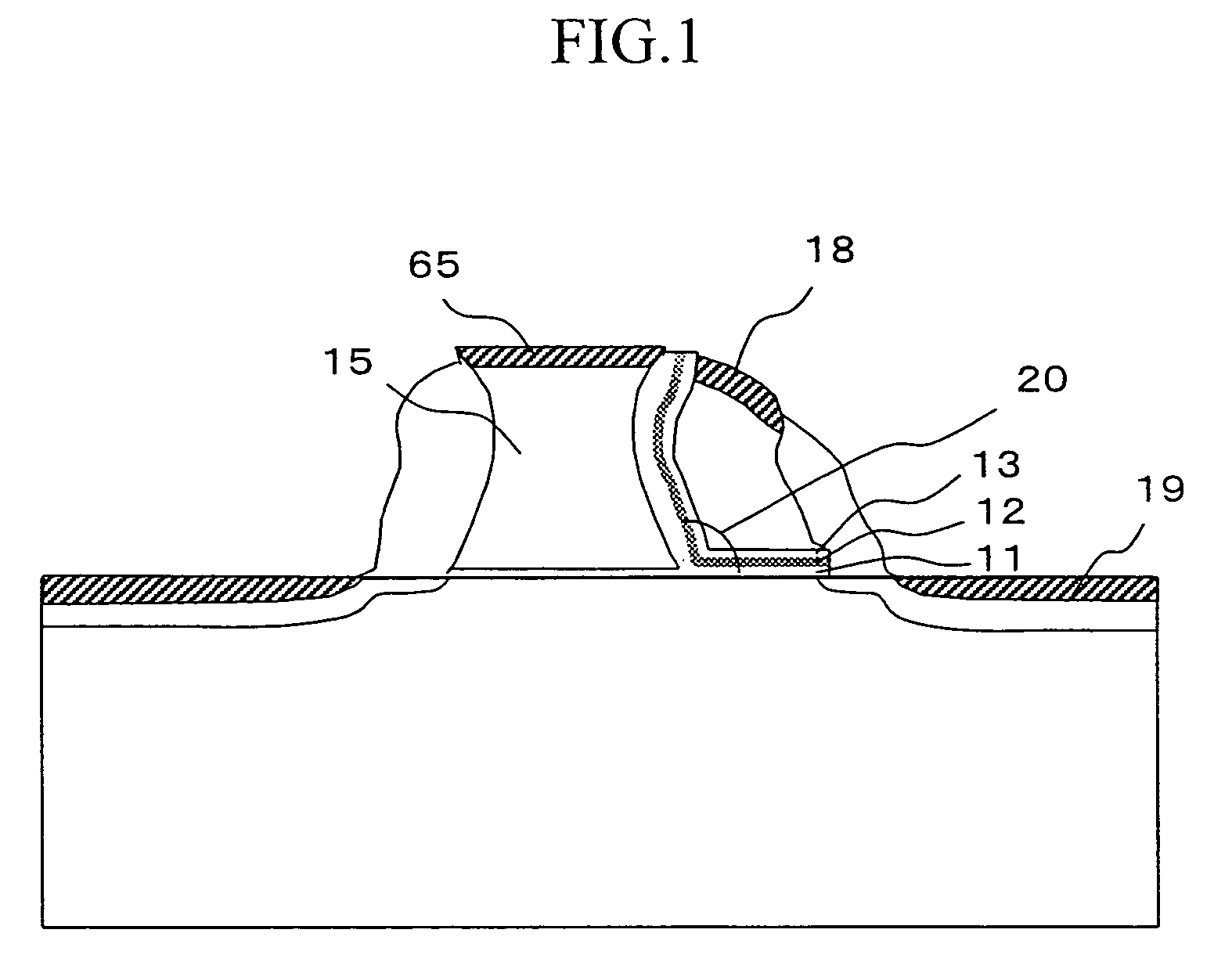
[0052]Next, a second embodiment of the present invention will be described with reference to FIG. 4. In this embodiment, the manufacturing method in which the sidewall of the select gate electrode is recessed so as to stably perform the silicide process of the gate electrode will be described.

[0053]The description which overlaps with that of the first embodiment will be appropriately omitted. The process equal to that of the first embodiment shown in an explanatory diagram of FIG. 6 is performed. Subsequently, a polysilicon film and a silicon oxide film are deposited in the same manner, and the silicon oxide film and the polysilicon film are removed by the dry etching with using a photoresist patterned by the photolithography as a mask, whereby the select gate electrode is formed. In this process, the dry etching of the polysilicon sidewall is performed under the condition that the isotropic component is increased. By so doing, the sidewall is recessed as shown in FIG. 4. The recess...

third embodiment

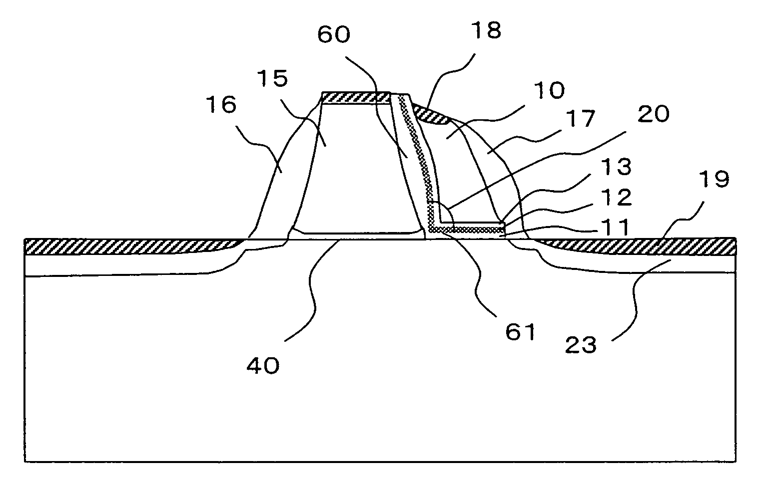
[0060]In this embodiment, the case where a step (convex portion) is provided between the select gate electrode and the self-aligned electrode so as to surely prevent the short-circuit in the silicide process will be described.

[0061]Since the process until the select gate electrode and the ONO film are formed is identical to that in the second embodiment, the description thereof will be omitted. Subsequently, a polysilicon film doped with an impurity to be the self-aligned electrode is deposited. The deposition thickness of the polysilicon film determines the gate length of the self-aligned electrode. The thickness is preferably within the range of 50 to 120 nm, and a polysilicon film with a thickness of 70 nm is deposited in this embodiment. When this polysilicon film is etched back by the anisotropic etching to form the self-aligned electrode, the over etching amount is increased to provide the step. It is preferable that the over etching of 20 to 80 nm is performed from the just e...


PUM


Abstract

In a split gate type nonvolatile memory cell in which a MOS transistor for a nonvolatile memory using a charge storing film and a MOS transistor for selecting it are adjacently formed, the charge storing characteristic is improved and the resistance of the gate electrode is reduced. In order to prevent the thickness reduction at the corner portion of the charge storing film and improve the charge storing characteristic, a taper is formed on the sidewall of the select gate electrode. Also, in order to stably perform a silicide process for reducing the resistance of the self-aligned gate electrode, the sidewall of the select gate electrode is recessed. Alternatively, a discontinuity is formed between the upper portion of the self-aligned gate electrode and the upper portion of the select gate electrode.

Description

CROSS-REFERENCE TO RELATED APPLICATION[0001]The present application claims priority from Japanese patent application No. JP 2003-359280 filed on Oct. 20, 2003, the content of which is hereby incorporated by reference into this application.BACKGROUND OF THE INVENTION[0002]The present invention relates to a nonvolatile semiconductor memory device and a manufacturing technique thereof. More particularly, the present invention relates to a technique effectively applied to a nonvolatile semiconductor memory device embedded on the same substrate along with a semiconductor device having a logic operating function, for example, a microcomputer.[0003]By embedding a semiconductor nonvolatile memory cell on the same silicon substrate along with a logic semiconductor device, a high-performance semiconductor device can be formed. Such a semiconductor device is widely used as an embedded microcomputer in industrial equipment, household appliances, and in-vehicle equipment, etc. Usually, the nonvo...

Claims


Application Information

Patent Timeline
Patent Type & Authority Patents(United States)
IPC IPC(8): H01L21/336H01L21/28H01L21/3205H01L21/4763H01L21/8246H01L21/8247H01L27/115H01L29/423H01L29/788H01L29/792
CPCH01L21/28273H01L21/28282H01L27/115H01L27/11521H01L27/11568H01L29/4232H01L29/792H01L29/40114H01L29/40117H10B43/30H10B69/00H10B41/30
Inventor YASUI, KANHISAMOTO, DIGHKIMURA, SHINICHIRO
Owner RENESAS ELECTRONICS CORP
Why Eureka
Try Eureka