Circuit board having electrically conductive structure formed between circuit layers thereof and method for fabricating the same

a technology of electrical conductivity and circuit layers, which is applied in the direction of conductive pattern reinforcement, resist details, conductive pattern formation, etc., can solve the problems of unreliable plated copper technique known in the prior art, no conduction or ineffective conduction and dramatic reduction of the production yield of the build-up circuit board. , to achieve the effect of simplifying the fabrication process, improving the quality of electrical connections, and reducing fabrication costs

Inactive Publication Date: 2007-08-07
PHOENIX PRECISION TECH CORP
View PDF6 Cites 9 Cited by
  • Summary
  • Abstract
  • Description
  • Claims
  • Application Information

AI Technical Summary

Benefits of technology

[0018]The circuit board having the electrically conductive structure formed between neighboring circuit layers thereof, proposed in the present invention, is fabricated by several distinct electroplating processes. First, the first patterned circuit layer is formed on an insulating layer of the circuit board by electroplating. Then, the conductive post is formed on the conductive pad of the first patterned circuit layer by electroplating to allow the thickness of the extension portion subsequently formed on the conductive post to be reduced. The second patterned circuit layer having the extension portion is formed on the conductive post by electroplating with the extension portion electrically connected to the conductive post. Thereby the via hole between neighboring circuit layers of the circuit board is filled up by several distinct electroplating processes, making the via hole completely filled with the filling material that is compactly deposited in the via hole, and also assuring the electrical connection between the circuit layers of the circuit board. Moreover, the height of the conductive post in the present invention can be adjusted to miniaturize the thickness of the extension portion, for the electrical connection use, subsequently formed on the conductive post, thereby improving the quality of electrical connection between neighboring circuit layers of the circuit board, and also simplifying the fabrication processes and reducing the fabrication cost as not requiring specific equipment or filling agent. As a result, the drawbacks of the prior art can be eliminated, and the production yield and reliability of the circuit board in the present invention are improved.

Problems solved by technology

Therefore, the plated filled copper technique known in the prior art is unreliable and leads to no conduction or ineffective conduction of the build-up circuit board.
The production yield of the build-up circuit board is dramatically reduced as the precision of the fabrication cannot be absolutely achieved.
However, since the insulating layer is relatively thick and the via hole is relatively deep, the above conventional plating-filled-copper process usually fails to completely fill the via hole with electroplated copper, such that the fabricated conductive via is not reliable and the electrical connection between the circuit layers in the circuit board through the conductive via may be defective, thereby degrading the production yield of the circuit board.
On the other hand, a normal copper-plating solution (such as copper sulfate, sulfuric acid and hydrochloric acid) is not suitable for the above plating-filled-copper process.
The superfilling copper-plating solution usually contains certain additives and thus is expensive in preparation, which thereby undesirably increases the fabrication cost.

Method used


Image

  • Circuit board having electrically conductive structure formed between circuit layers thereof and method for fabricating the same
  • Circuit board having electrically conductive structure formed between circuit layers thereof and method for fabricating the same
  • Circuit board having electrically conductive structure formed between circuit layers thereof and method for fabricating the same

Examples


Embodiment Construction

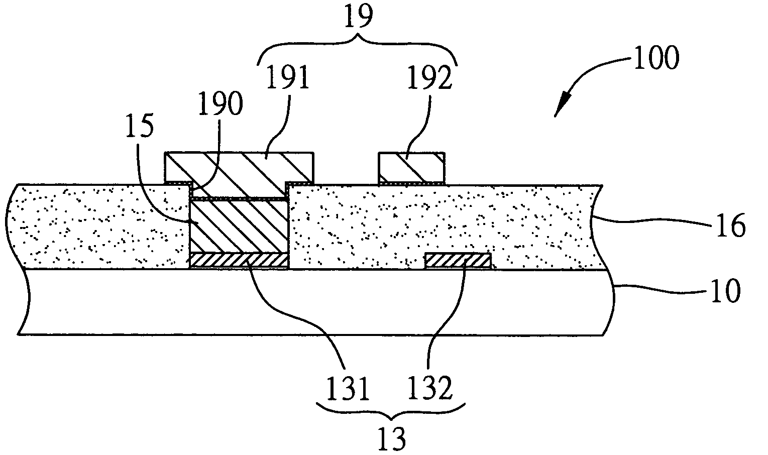
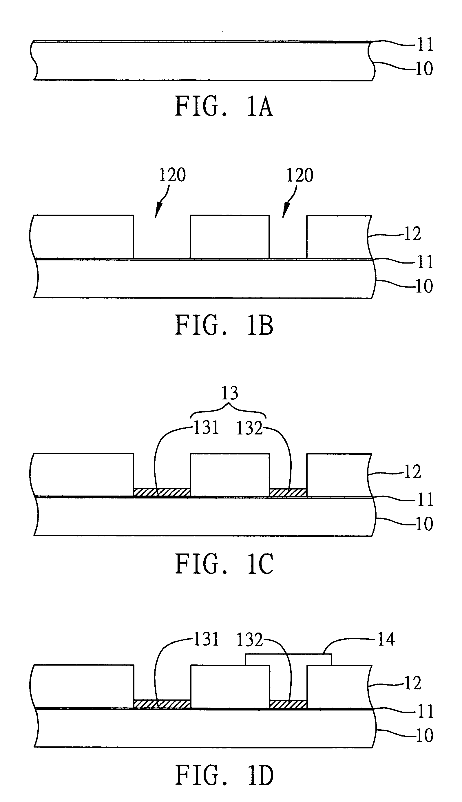
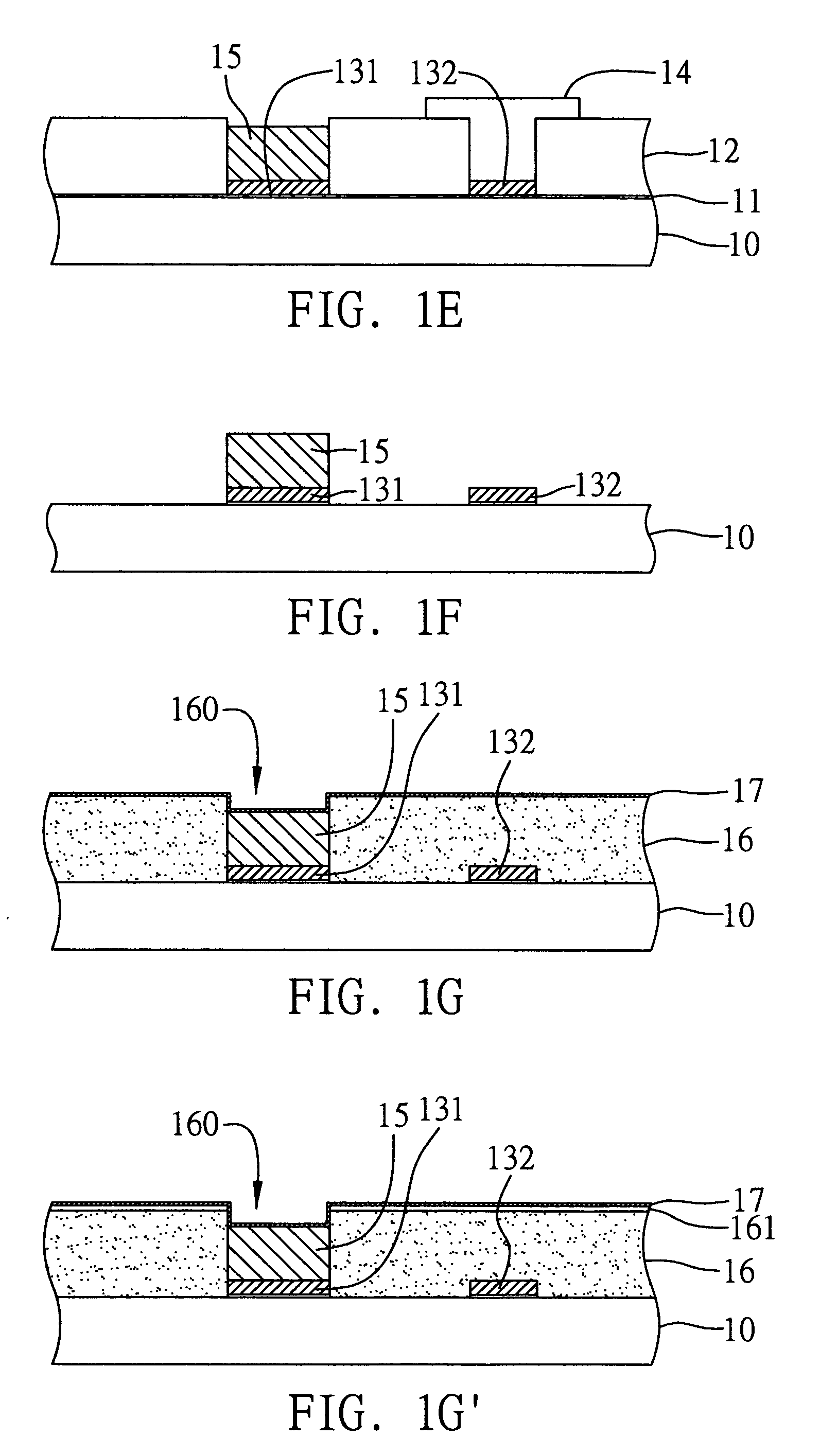
[0022]The preferred embodiment of a method for fabricating a circuit board having an electrically conductive structure formed between circuit layers thereof proposed in the present invention is described in detail with reference to FIGS. 1A to 1J.

[0023]Referring first to FIG. 1A, a dielectric insulating layer 10 is prepared with a first conductive layer 11 formed thereon. The dielectric insulating layer 10 can be made of a material such as epoxy resin, polyimide resin, cyanate ester, glass fiber, bismaleimide triazine (BT) resin, or a mixture (FR5) of epoxy resin and glass fiber. The dielectric material layer can be formed on the core substrate that has at least one patterned circuit layer thereon. The first conductive layer 11 primarily serves as a current conductive path for a subsequent electroplating process. The first conductive layer 11 can be made of a metal, an alloy, or several laminated metal layers, selected from Copper (Cu), Tin (Sn), Nickel (Ni), Chromium (Cr), Titanium...


PUM

PropertyMeasurementUnit
electrically conductiveaaaaaaaaaa
diameteraaaaaaaaaa
conductiveaaaaaaaaaa

Abstract

A circuit board and a fabrication method thereof. Providing the insulating layer with a first conductive layer formed thereon; wherein the insulating layer was formed on a core substrate with at least one patterned circuit layer thereon. A first resist layer is applied on a first conductive layer, forming first openings to expose the first conductive layer. A first patterned circuit layer, including conductive pads and traces, is formed in the first openings. A second resist layer is applied to cover the traces, and a conductive post is formed on each conductive pad. The first and second resist layers and the first conductive layer underneath the first resist layer are removed. A dielectric material layer is formed on the insulating layer with first patterned circuit layer, forming second openings to expose the conductive posts. A second conductive layer is formed on the dielectric material layer and in the second openings. A third resist layer is applied on the second conductive layer, forming third openings of the third resist layer to expose the second conductive layer. A second patterned circuit layer is formed in the second and third openings.

Description

FIELD OF THE INVENTION[0001]The present invention relates to circuit boards having electrically conductive structures between circuit layers thereof and methods for fabricating the same, and more particularly, to a circuit board having an electrically conductive structure formed between neighboring circuit layers by filling vias in the circuit board through the use of electroplating technology, and a fabrication method of the circuit board.BACKGROUND OF THE INVENTION[0002]Due to gradually reduced size of electronic products, semiconductor packages used in the electronic products are accordingly required having high density, high speed and low cost, such as flip-chip package; ball grid array (BGA) package, chip size package (CSP) and multi chip module (MCM) that become the mainstream packaging technology in the market.[0003]For flip-chip package, BGA package, CSP and MCM, the build-up technology for fabricating circuit boards is popularized and cost-effective to implement, making the...

Claims


Application Information

Patent Timeline
Patent Type & Authority Patents(United States)
IPC IPC(8): H05K1/11H01R12/04C25D5/02H05K3/10H05K3/24H05K3/46
CPCC25D5/022H05K3/4647H05K3/108H05K3/243H05K2203/0574H05K2203/0733
Inventor TANG, SAO-HSIAWANG, SHING-RU
Owner PHOENIX PRECISION TECH CORP
Why Eureka
Try Eureka