Data processing device

a data processing and data technology, applied in the field of data processing devices, can solve the problems of power source noise and nonvolatile memory malfunction, and achieve the effects of preventing relatively large power source noise, reducing delay, and reducing power source nois

Active Publication Date: 2007-08-07
RENESAS ELECTRONICS CORP
View PDF5 Cites 16 Cited by
  • Summary
  • Abstract
  • Description
  • Claims
  • Application Information

AI Technical Summary

Benefits of technology

[0004]The present inventors have studied rewritable nonvolatile memory of 1 transistor / 1 bit. First, when boost forming a rewriting negative voltage therein, the present inventors have studied the stop of the booster in a low power consumption mode from the viewpoint of low power consumption. When stopping the booster, a circuit node at a negative voltage becomes a circuit ground voltage. When releasing the low power consumption mode, boosting operation is restarted from the beginning. The present inventors have proved that the start of the later read operation is delayed. Second, in driving an unselected word line to a negative voltage such as −2V and a selected word line to a voltage such as 0V by a word driver in read operation, when inverting a word line voltage by the word driver, the inverting speed depends on the charging ability and the discharging ability of the word driver. When they are not balanced, the access time of read operation is matched with the operation of the slower one. The present inventors have revealed that when there is an unignorable significant difference between Vgs (gate-source voltage) when an n-channel MOS transistor of a CMOS inverter is turned on and Vgs when a p-channel MOS transistor of the CMOS inverter is turned on, the employment of an output circuit like the CMOS inverter for the output stage of the word driver is not enough. Third, the present inventors have made it apparent that when the operating speed switching application of a high voltage or a source voltage is too high in write operation and erase operation, a relatively large electric current is abruptly flowed to cause power source noise. Such power source noise can cause malfunction of nonvolatile memory and a data processing device over which the same is mounted. Fourth, when applying a high voltage to bit lines at write and erase, the bit lines need be selectively isolated from a read system connected to a sense amplifier. A high voltage MOS transistor having a thick gate oxide film is employed for such an isolating circuit. The present inventors have found that an undesired resistance component in a read path is increased in read operation to lower the read speed of stored information.
[0005]A representative object of the present invention is to reduce a delay from the release of a low power consumption mode of nonvolatile memory to the restart of read operation.
[0006]Another representative object of the present invention is to make the inverting operation of a word line voltage of a word driver in nonvolatile memory fast.

Problems solved by technology

Third, the present inventors have made it apparent that when the operating speed switching application of a high voltage or a source voltage is too high in write operation and erase operation, a relatively large electric current is abruptly flowed to cause power source noise.
Such power source noise can cause malfunction of nonvolatile memory and a data processing device over which the same is mounted.
Fourth, when applying a high voltage to bit lines at write and erase, the bit lines need be selectively isolated from a read system connected to a sense amplifier.

Method used


Image

  • Data processing device
  • Data processing device
  • Data processing device

Examples


Embodiment Construction

>

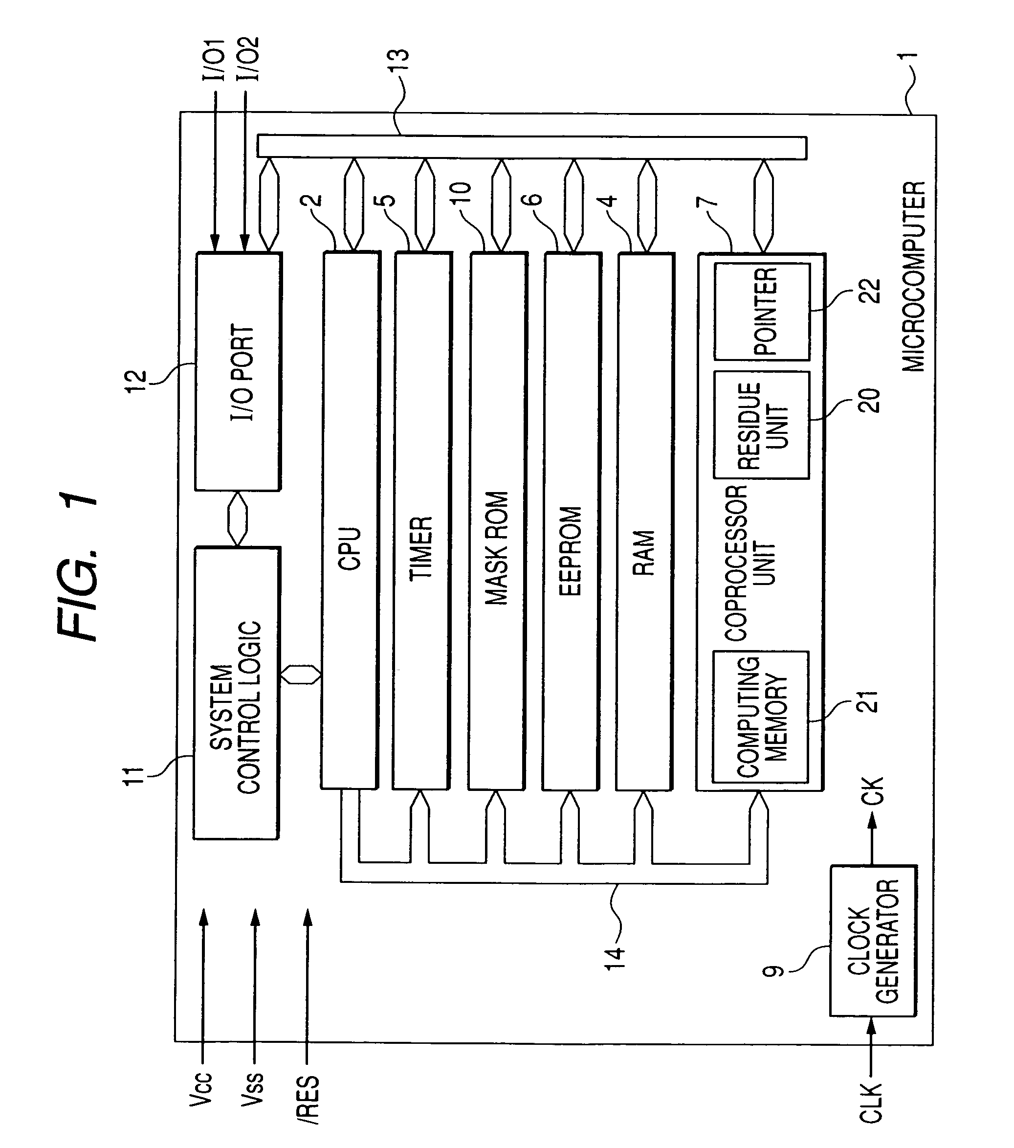
[0052]FIG. 1 shows a microcomputer as an example of a data processor. A microcomputer 1 shown in the drawing, not being particularly limited, is a microcomputer for an IC card called an IC card microcomputer. The microcomputer 1 shown in the drawing is formed over one semiconductor substrate or semiconductor chip such as single crystal silicon by the data processing device manufacturing technique such as CMOS.

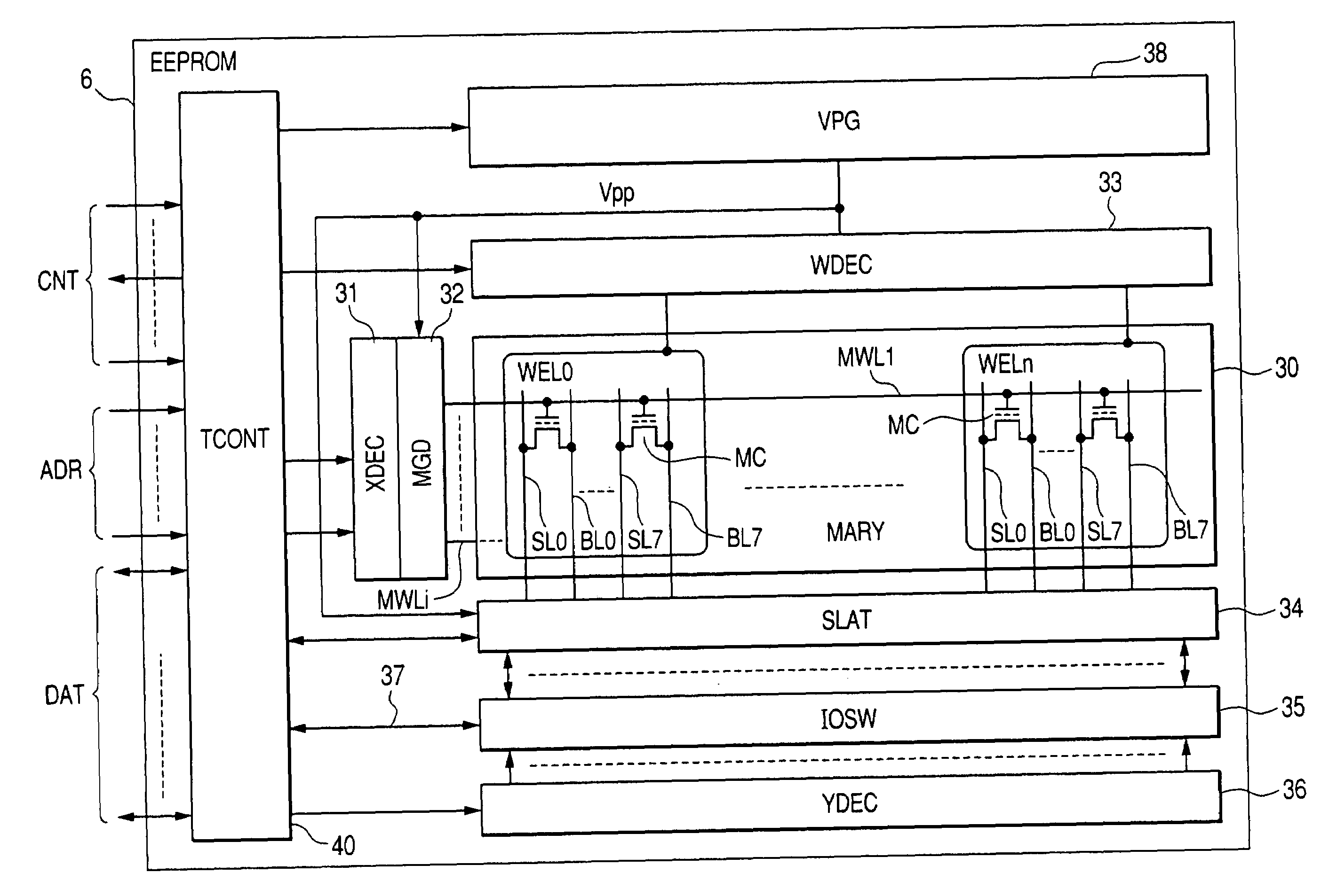
[0053]The microcomputer 1 has a central processing unit (CPU) 2, random access memory (RAM) 4, a timer 5, EEPROM (electrically erasable and programmable read only memory) 6, a coprocessor 7, a clock generator 9, mask ROM 10, a system control logic 11, an input / output port (I / O port) 12, a data bus 13, and an address bus 14.

[0054]The EEPROM 6 is used for storing data employed in computing processing of the CPU 2. The mask ROM is used for storing a program (operating program) executed by the CPU 2. The RAM 4 is a work area of the CPU 2 or a temporary storage area of data and is ...


PUM


Abstract

A delay from the release of a low power consumption mode of nonvolatile memory to the restart of read operation is reduced. Nonvolatile memory which can electrically rewrite stored information has in well regions plural nonvolatile memory cell transistors having drain electrodes and source electrodes respectively coupled to bit lines and source lines and gate electrodes coupled to word lines and storing information based on a difference between threshold voltages to a word line select level in read operation, and the nonvolatile memory has a low power consumption mode. In the low power consumption mode, a second voltage lower than a circuit ground voltage and higher than a first negative voltage necessary for read operation is supplied to the well regions and word lines. When boost forming a rewriting negative voltage therein, a circuit node at a negative voltage is not the circuit ground voltage in the low power consumption mode.

Description

CROSS-REFERENCE TO RELATED APPLICATION[0001]The present application claims priority from Japanese patent application No. 2004-345688 filed on Nov. 30, 2004, the content of which is hereby incorporated by reference into this application.BACKGROUND OF THE INVENTION[0002]The present invention relates to a data processing device having nonvolatile memory which can electrically rewrite stored information. For instance, the present invention relates to a technique effective to be applied to EEPROM (electrically erasable and programmable read only memory) employing an on-chip MONOS (metal oxide nitride oxide semiconductor) type memory cell of 1 transistor / 1 bit of a microcomputer for an IC card.[0003]A nonvolatile memory transistor which can electrically rewrite stored information has a channel forming region between a source electrode and a drain electrode and a charge storage region (trap region) storing electric charges such as electrons or holes via a gate oxide film over the channel f...

Claims


Application Information

Patent Timeline
Patent Type & Authority Patents(United States)
IPC IPC(8): G11C5/14G11C16/04G11C16/06
CPCG11C16/0466G11C16/08G11C16/10G11C16/32
Inventor TERASAWA, MASAAKIKAWAJIRI, YOSHIKIYAMAZOE, TAKANORI
Owner RENESAS ELECTRONICS CORP
Why Eureka
Try Eureka