Flexible electronic device and production method of the same

a technology of electronic devices and production methods, applied in the direction of laminating printed circuit boards, non-linear optics, instruments, etc., can solve the problems of increasing production costs, card bending force, and damage to chips, and achieves excellent heat liberation characteristics and toughness, low cost, and high reproducibility.

Active Publication Date: 2007-09-18
HANNSTAR DISPLAY CORPORATION
View PDF16 Cites 11 Cited by
  • Summary
  • Abstract
  • Description
  • Claims
  • Application Information

AI Technical Summary

Benefits of technology

[0010]An object of the present invention is to provide flexible electronic devices such as flexible IC devices, flexible display devices and the like, excellent in heat liberation characteristics and toughness, and a method for producing these devices with low costs and high reproducibility.
[0011]A flexible electronic device of the present invention is a flexible electronic device in which on a flexible film, a substrate is situated which is different in material from the film, and a thin film device is formed on the substrate, wherein the thickness of the substrate is larger than 0 μm and not larger than 200 μm. As the flexible films of the flexible electronic devices of the present invention, there can be used insulating flexible films such as polyethylene terephthalate (PET) film, high thermal conductivity films having larger thermal conductivities than those of glasses, such as copper film and gold film and optically functional films such as polarizing films and phase difference films. As the flexible films, there can be used a film having a laminated structure composed of an insulating flexible film and a high thermal conductivity film. The use of the high thermal conductivity films such as copper film and gold film having larger thermal conductivities than those of glasses, as the flexible films for the flexible electronic devices of the present invention, permits suppressing the deterioration in characteristics of the thin film devices caused by self-heating.
[0012]Additionally, the production method of the flexible electronic devices of the present invention can produce a flexible electronic device as follows: a substrate on which an electronic device such as a thin film transistor array is formed is subjected to etching from the, back surface (the substrate surface opposite to the surface for electronic device formation) until the residual thickness of the substrate becomes larger than 0 μm and not larger than 200 μm, and thereafter a flexible film is adhered onto the etched surface to produce a flexible electronic device. The production method of the flexible electronic device of the present invention can regulate the residual thickness of the substrate to a desired value with high reproducibility within the range larger than 0 μm and not larger than 200 μm.
[0013]The production method of the flexible electronic device of the present invention provides the following advantages.
[0014](1) A protection film adhered to the device surface can be easily peeled so that the throughput is not degraded in contrast to the conventional techniques.

Problems solved by technology

Usually these IC cards are often carried in wallets and the like, and the cards are frequently subjected to bending forces caused by the movements of the carriers.
However, conventional IC chips, namely, semiconductor chips themselves formed with silicone wafer are not flexible, and moreover, are relatively fragile, and hence there is a high possibility that these chips will be damaged when external forces are exerted thereon.
Among the above described conventional techniques, in Japanese Patent Laid-Open No. 9-312349, a step of peeling a semiconductor IC chip from a silicon wafer and a-step of transferring onto a flexible resin sheet are low in yield to thereby raise the production cost.
Additionally, the IC chip is of the order of a few tens μm in thickness and is not transparent so that the applicable areas thereof are limited and the element isolation of the active elements (for example, transistors) is complicated in such a way that mixed loading of high voltage elements and low voltage elements becomes difficult.
The multilayer composite boards disclosed in Japanese Patent Laid-Open No. 2002-111222 and Japanese Patent Laid-Open No. 2002-111226 have semiconductor IC chips, formed of silicon wafer, mounted on resin substrates and thus raise the production costs.
Additionally, it has become obvious that these semiconductor IC chips suffer from deterioration in characteristics caused by self-heating.
Furthermore, in the technique in which transferring is made onto a resin substrate after the glass portion has been completely removed from the back surface thereof by etching or polishing a glass substrate on which a thin film transistor array is formed, for the purpose of forming flexible liquid crystal display devices, the step of peeling the protection sheet, illustrated in FIG. 1D, requires a fairly long period of time for successfully transferring the thin film transistor array onto the resin substrate, and hence the throughput concerned is remarkably degraded.
Additionally, the step of forming an etching stopper layer as a film is to be added, which raises the costs.

Method used


Image

  • Flexible electronic device and production method of the same
  • Flexible electronic device and production method of the same
  • Flexible electronic device and production method of the same

Examples


first embodiment

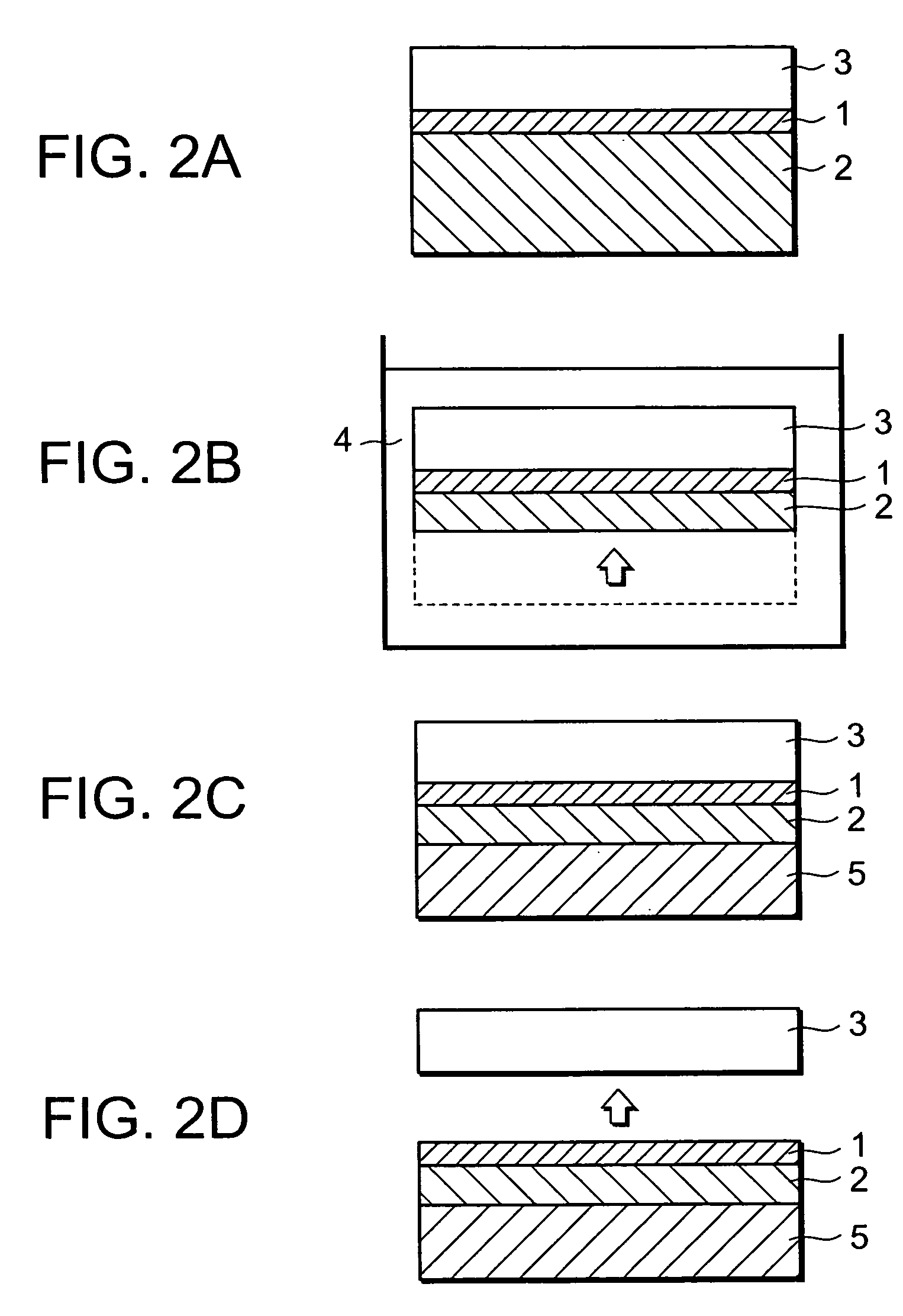
[0031]FIGS. 2A to 2D are the schematic sectional views illustrating a production method of a flexible electronic device involved in the present invention. As FIG. 2A shows, a protection film 3 is adhered onto the device formation surface (the front surface) of a glass substrate 2 on which a thin film device 1 is formed. Successively, as FIG. 2B shows, the substrate 2 is subjected to etching from the back surface by soaking in an etching solution 4. On the basis of the etching rate determined beforehand, the etching is terminated when a desired residual thickness of the substrate is reached. Thus, the residual thickness is made to be larger than 0 μm and not larger than 200 μm. In this connection, it should be noted that if the residual thickness of the substrate 2 vanishes, the characteristics of the thin film device are degraded, and if the residual thickness is larger than 200 μm, no sufficient flexibility can be achieved. Furthermore, as FIG. 2C shows, a flexible film 5 is adhere...

second embodiment

[0033]Now, description will be made below on the present invention.

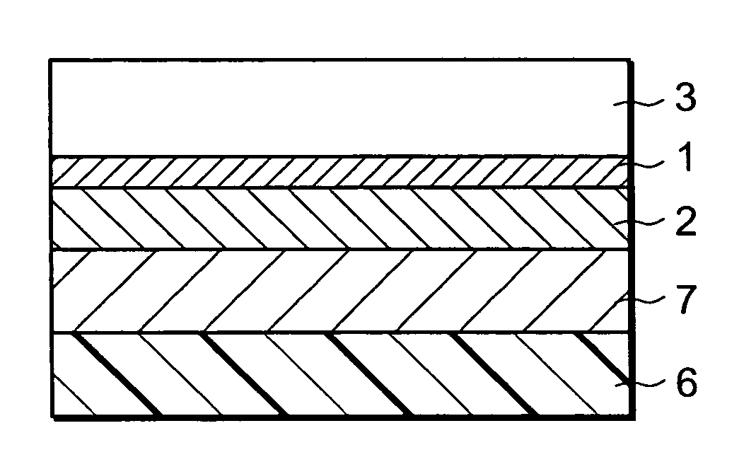
[0034]FIGS. 3A and 3B illustrate the second embodiment. FIG. 3A illustrates a case where in place of the flexible film 5 in FIG. 2C, a highly thermally conductive film 6 having a thermal conductivity higher than 0.01 W / cm·deg is used, while FIG. 3B illustrates a case where in place of the flexible film 5 in FIG. 2C, a laminated film made of an insulating flexible film 7 and the highly thermally conductive film 6. The vertical order of the insulating flexible film 7 and the highly thermally conductive film 6 may be reversed. In this connection, the value of 0.01 W / cm·deg refers to a thermal conductivity of a glass, and the use of a film having a thermal conductivity higher than this value improves the heat liberation characteristics of a flexible thin film transistor device. As examples, a copper film (thermal conductivity=4.0 W / cm·deg) and a gold film (thermal conductivity=2.3 W / cm·deg) were used as the highly therma...

third embodiment

[0036]Now, description will be made below on the present invention.

[0037]FIGS. 5A to 5E show a production method of a flexible display device involved in the third embodiment. As FIG. 5A shows, at the beginning, a protection film 11 is adhered onto a glass plate 9 of a display device having a structure in which a display element 8 is sandwiched between a pair of a glass substrate 9 and a glass substrate 10. Successively, as FIG. 5B shows, the thus treated display device is soaked in a hydrofluoric acid based etching solution 12 to etch the glass substrate 10. On the basis of the etching rate determined beforehand for the glass substrate 10, the etching is terminated when the residual thickness of the glass substrate 10 reaches a desired value. The residual thickness of the glass substrate 10 is adjusted to be larger than 0 μm and not larger than 200 μm. Then, as FIG. 5C shows, a flexible film 13 is adhered onto the etched surface of the glass substrate 10, and the protection film 11...


PUM

PropertyMeasurementUnit
thicknessaaaaaaaaaa
thicknessaaaaaaaaaa
residual thicknessaaaaaaaaaa

Abstract

A flexible electronic device excellent in heat liberation characteristics and toughness and a production method for actualizing thereof in low cost and with satisfactory reproducibility are provided. A protection film is adhered onto the surface of a substrate on which surface a thin film device is formed. Successively, the substrate is soaked in an etching solution to be etched from the back surface thereof so as for the residual thickness of the substrate to fall within the range larger than 0 μm and not larger than 200 μm. Then, a flexible film is adhered onto the etched surface of the substrate, and thereafter the protection film is peeled to produce a flexible electronic device.

Description

BACKGROUND OF THE INVENTION[0001]1. Field of the Invention[0002]The present invention relates to a flexible electronic device and a production method of the same. In particular, the present invention relates to a method for producing a flexible silicon electronic device and a flexible liquid crystal display device.[0003]2. Description of the Prior Art[0004]In these years, demand has grown for IC cards provided with a built-in memory circuit and a microprocessor circuit, as they have larger storage capacity compared with magnetic cards. Usually these IC cards are often carried in wallets and the like, and the cards are frequently subjected to bending forces caused by the movements of the carriers. However, conventional IC chips, namely, semiconductor chips themselves formed with silicone wafer are not flexible, and moreover, are relatively fragile, and hence there is a high possibility that these chips will be damaged when external forces are exerted thereon. For the purpose of preve...

Claims


Application Information

Patent Timeline
Patent Type & Authority Patents(United States)
IPC IPC(8): H01L29/04H01L29/15G02F1/1333G02F1/1368G06K19/077H01L21/02H01L21/336H01L27/12H01L29/786H05K1/00H05K3/00
CPCH01L29/78603H05K1/0393H05K3/002H05K3/0058Y10T428/1014H01L2924/0002Y10T428/1086H01L2924/00C09K2323/023C09K2323/06H01L27/1266
Inventor TAKECHI, KAZUSHIGE
Owner HANNSTAR DISPLAY CORPORATION
Why Eureka
Try Eureka