
Microelectromechanical systems using thermocompression bonding

a technology of thermocompression bonding and microelectromechanical systems, which is applied in the direction of fluid speed measurement, instruments, coatings, etc., can solve the problems of microelectromechanical devices, mems devices are even more vulnerable to contamination and moisture, and cannot be encapsulated in a typical injection-molded plastic package, so as to reduce parasitics, reduce parasitic capacitance, and small electrical interconnections formed with the invention

Inactive Publication Date: 2007-10-02
MICROASSEMBLY TECH
View PDF31 Cites 53 Cited by
  • Summary
  • Abstract
  • Description
  • Claims
  • Application Information

AI Technical Summary

Benefits of technology

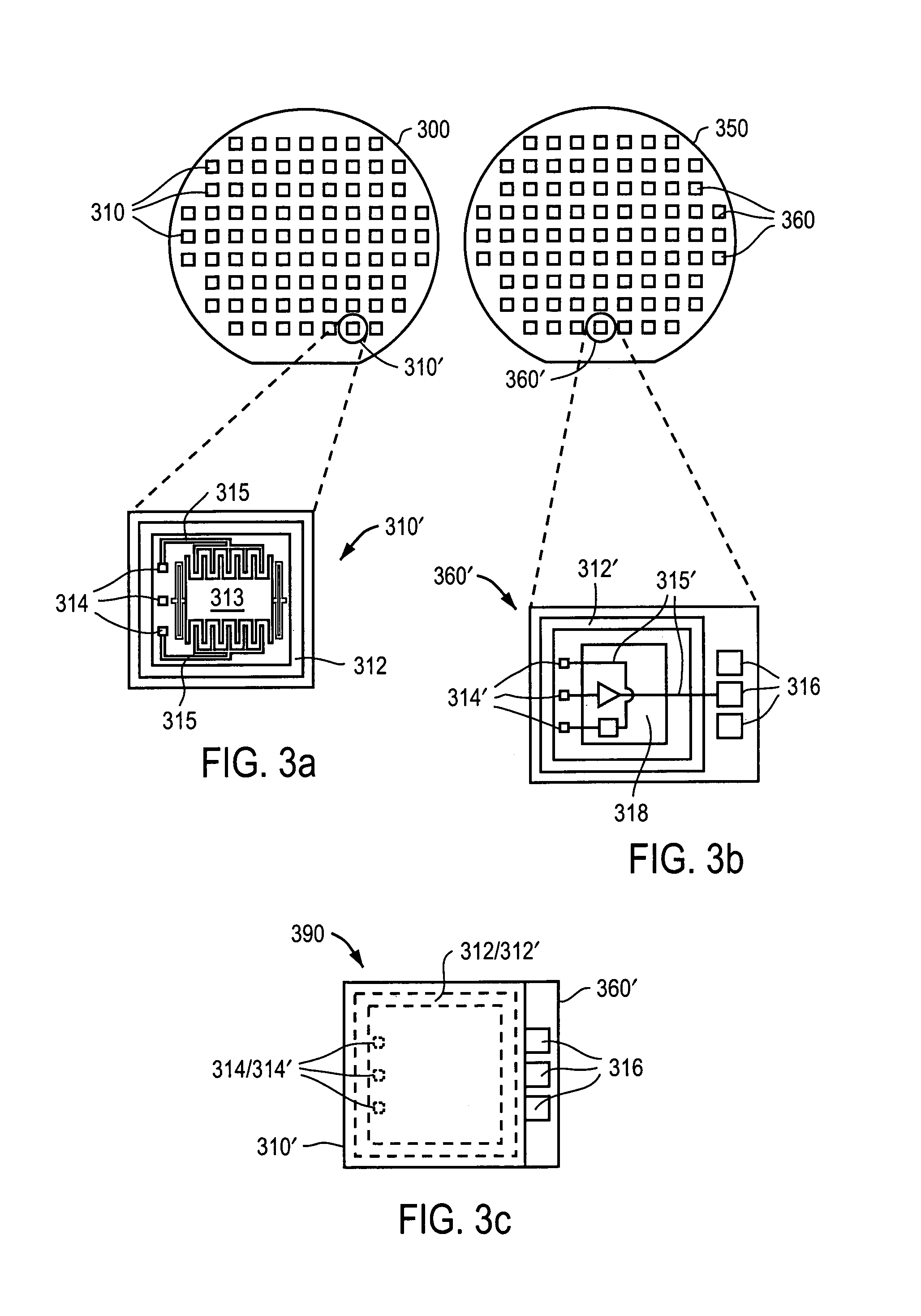
"The present invention provides methods and apparatus for thermocompressively bonding plural substrates with various structures, such as microelectromechanical devices and integrated circuits, to create bonded hybrid structures. These methods and apparatus allow for the bonding of wafers and chips on a wafer-scale or chip-scale, and can include the use of conductive bonding material, such as electroplated gold or copper, and target features formed during fabrication of the substrates. The resulting bonded structures provide a sealed cavity that protects the microelectromechanical devices and ensures electrical coupling between the devices and the integrated circuit. The invention also includes bonded hybrid structures with MEMS devices and integrated circuits, as well as methods for eliminating wire-bond pads and directly connecting conductive lines to the thermocompression bonds."

Problems solved by technology

Although they are generally fabricated on silicon wafers, these “microelectromechanical devices” or “MEMS” are different from most ICs in that they possess moving elements.
Although MEMS devices are even more vulnerable to contamination and moisture than most ICs, they cannot be encapsulated in a typical injection-molded plastic package because at least one element of every microelectromechanical device must remain free to move.
The packaging of MEMS devices, therefore, presents unique problems.
One problem with this chip-scale packaging approach is the expense associated with handling the individual components (e.g., the packages, lids, etc.) and assembling them into a single package.
An additional problem with this chip-scale packaging approach is that the moving elements in MEMS are extremely fragile and tend to be damaged by any handling, especially near the end of the fabrication process.
Therefore, packaging yields are typically low.
A further problem with this packaging approach is that the solder seal on the lid tends to outgas when reflowed during the final sealing process.
If a vacuum is needed inside the package, a getter must be added, at additional cost.
In such cases, packaging costs can constitute 80% of the total device cost.
In sum, the use of ceramic packages to seal and package MEMS chips is inordinately expensive due to the need to individually handle components, the need to use getters and the considerable opportunity for damage and contamination of the MEMS devices.
While this process has been marginally successful, it suffers from the deficiency that the glass frit cannot be patterned into fine features.
Attempts have been made to improve the glass frit patterning resolution, using lithographic methods, but these have not shown success.
Further, gasket patterns thinner than 100–200 microns in width do not appear to provide reliable hermetic seals, possibly because of the inherently porous nature of glass frits.
Thus, it is currently believed that glass frit techniques simply cannot be applied on a smaller scale where hermetic seals are desired.
One drawback of using such a high firing temperatures is that it effectively precludes the incorporation of integrated circuitry on either of the wafers bonded together.
Such high temperatures also damage the MEMS themselves and, particularly, certain structural films deposited at lower temperatures and structures in which the film stress must be carefully controlled.
Another deficiency of glass frit techniques is that the glass frit itself employs organic binders, which outgas into the sealed cavity during firing.
Since getters are not available to combat this problem, this fact precludes the use of glass frits for vacuum applications.
Still another limitation of the glass frit techniques is that the sealing materials, being non-conductive, cannot be used to establish electrical coupling between the devices disposed on the bonded substrates.
However, these processes have low throughput and require high temperatures for high-quality bonds because their bonding mechanisms involve solid diffusion across the bond interface.
These methods also place strict constraints on the materials and processes used to form the wafers to be bonded together.
Significantly, these methods are also exceptionally sensitive to the presence of even small particulate contaminants, wafer warpage, scratches, and other imperfections commonly encountered during semiconductor fabrication because such contaminants can cause large defects in the bond and reduce yield substantially.
Moreover, normal variations in surface topology due to the presence of circuitry can preclude proper bonding and / or sealing using such methods.
The use of solder to form a seal is not compatible with present MEMS process technologies because MEMS are easily damaged by residual solder flux left after sealing has occurred.
While fluxless soldering processes have been attempted, even this approach does not resolve an inherent real-estate inefficiency problem resulting from the fact that the minimum feature size of this solder-based technology is about 100 microns.
Yet another problem with solder-based flip-chip bonding is that special processing is required; not only for fabrication of the solder structures on the lid chip, but also to coat the appropriate areas of the microsensor chip with a solderable metal.
Since some standard metals used by commercial IC foundries cannot be soldered directly, solder-based flip-chip technology is still expensive and of limited utility compared to the present invention.
Finally, solder-based flip-chip bonding cannot be reliably performed on a wafer-scale because, for example, the normal curvature of processed wafers can exceed the solder bump height.
For all of the reasons above, this chip-scale technique is disproportionately expensive relative to wafer-scale packaging / sealing techniques.
Possibly, this is because manufacturers have confined themselves to standard packaging techniques, such as wirebonding, flip-chip, etc.
For these reasons, gold is not allowed in wafer fabrication facilities.
Therefore, many manufacturers would be unlikely to use gold in their MEMS products.

Method used


Image

  • Microelectromechanical systems using thermocompression bonding
  • Microelectromechanical systems using thermocompression bonding
  • Microelectromechanical systems using thermocompression bonding

Examples


Embodiment Construction

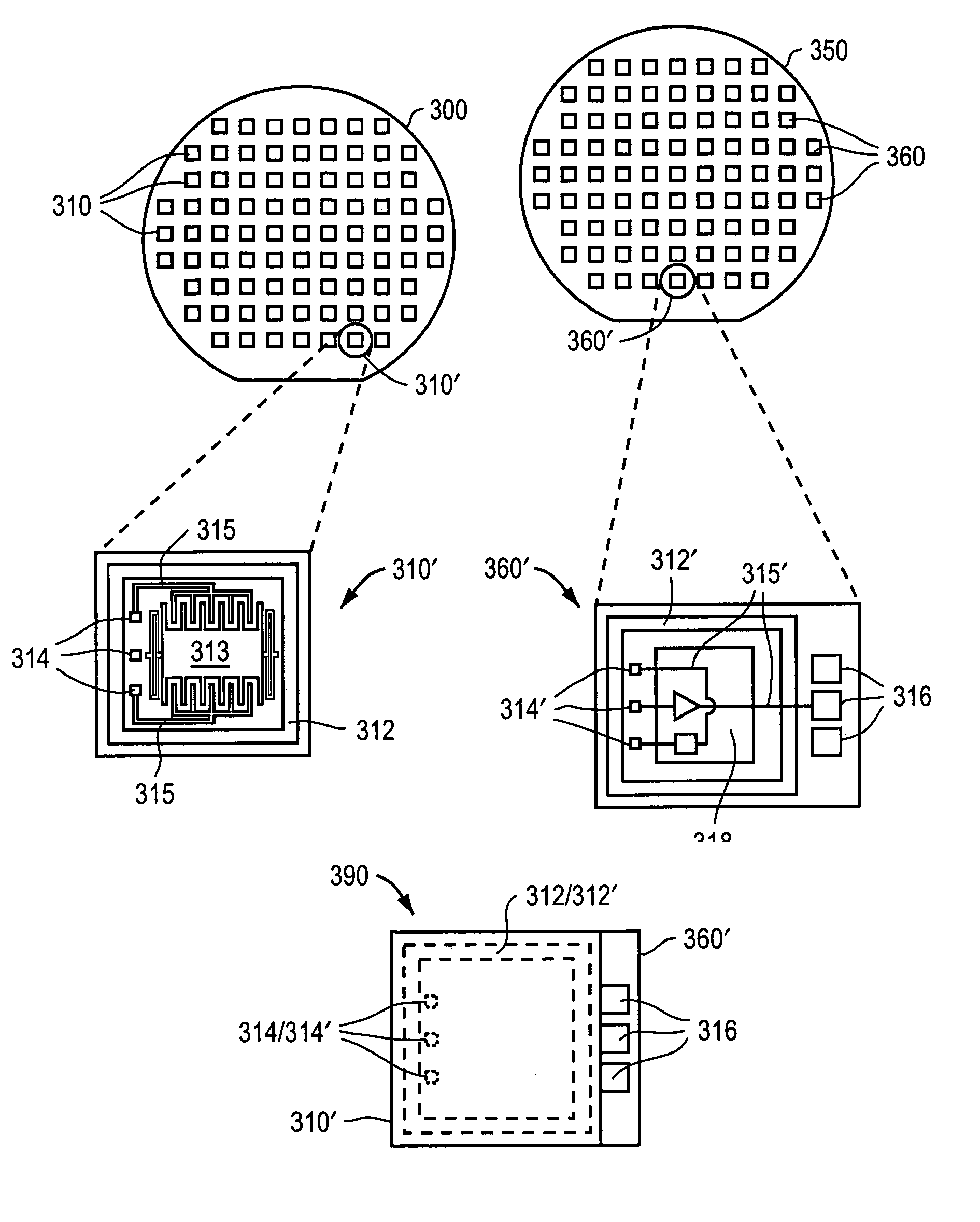
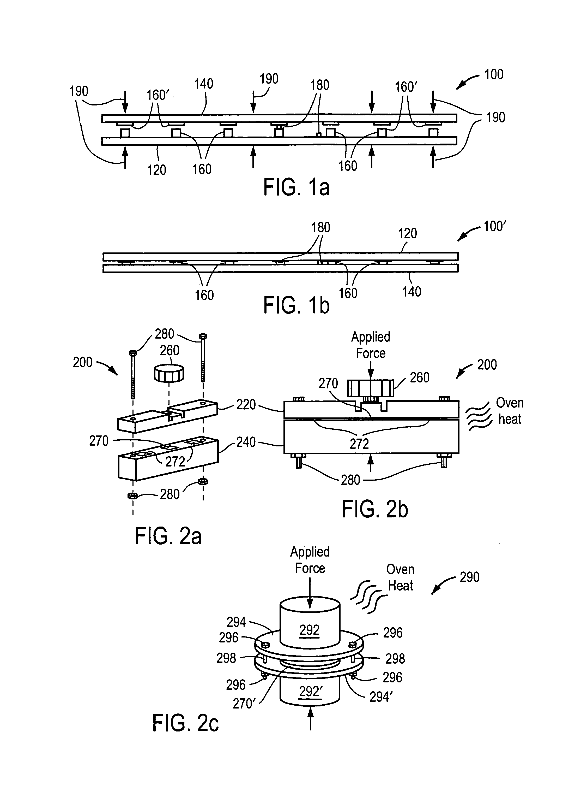
[0041]A cross-sectional view of an exemplary pair of substrates 100 in accordance with the invention are shown in FIGS. 1a and 1b, these Figures illustrating structures and principles of the invention applicable throughout the various embodiments of the invention. As shown in FIG. 1a, a first substrate 120 is preferably made of a relatively hard material (such as silicon, silicon dioxide, quartz, pyrex, glass, gallium arsenide or another material known in the art) and bears a plurality of bonding features 160 on an upper surface of substrate 120. These bonding features can assume virtually any desired dimension or shape such as contact bumps, lines and / or sealing rings and are disposed on predetermined locations of substrate 120. For example, the rings can be in the form of a continuous line or wall of substantially uniform thickness and height and may assume an annular (round or elliptical), rectangular, trapezoidal or square shape, etc., as viewed from above.

[0042]Further, bonding...


PUM

PropertyMeasurementUnit
heightaaaaaaaaaa
sizeaaaaaaaaaa
widthaaaaaaaaaa

Abstract

Improved microelectromechanical systems (MEMS), processes and apparatus using thermocompression bonding are disclosed. For example, process embodiments are disclosed in which wafer-scale as well as die-scale thermocompression bonding is utilized to encapsulate MEMS and / or to provide electrical interconnections with MEMS. Apparatus embodiments include apparatus for performing thermocompression bonding and bonded hybrid structures manufactured in accordance with the process embodiments. Devices having various substrate bonding and / or sealing configurations variously offer the advantage of reduced size, higher manufacturing yields, reduced costs, improved reliability, improved compatibility with existing semiconductor manufacturing process and / or greater versatility of applications.

Description

CROSS-REFERENCE TO RELATED APPLICATION[0001]This application is a continuation of U.S. patent application Ser. No. 10 / 377,999, filed Feb. 28, 2003, now patented and bearing U.S. Pat. No. 6,853,067, which is a divisional of U.S. patent application Ser. No. 09 / 687,480, filed Oct. 12, 2000, now abandoned, which claims the benefit of U.S. Provisional Application No. 60 / 159,026, filed Oct. 12, 1999.STATEMENT REGARDING FEDERALLY SPONSORED RESEARCH OR DEVELOPMENT[0002]This invention was made with Government support under Contract DAAH01-99-C-R038 awarded by the U.S. Army Aviation and Missile Command. The Government has certain rights in the invention.BACKGROUND OF THE INVENTION[0003]1. Field of the Invention[0004]The present invention relates to the packaging of semiconductor devices, and, more particularly, to the use of thermocompression bonding in the packaging of microelectromechanical systems (MEMS). Accordingly, the general objects of the invention are to provide novel methods and ap...

Claims


Application Information

Patent Timeline
Patent Type & Authority Patents(United States)
IPC IPC(8): H01L23/12B81B7/00B81C1/00H01L21/60H01L23/10
CPCB81C1/00238H01L23/10H01L24/75H01L24/81B81C2203/0109H01L2924/1461H01L2924/10253H01L2924/014H01L2924/01075H01L2924/01074H01L2924/0105B81C2203/0118B81C2203/019H01L2224/13111H01L2224/48095H01L2224/48137H01L2224/49175H01L2224/75H01L2224/7598H01L2224/81801H01L2924/01013H01L2924/01029H01L2924/01032H01L2924/01046H01L2924/01049H01L2924/01077H01L2924/01078H01L2924/01079H01L2924/01082H01L2924/14H01L2924/19041H01L2924/30105H01L2924/3011H01L24/48H01L24/49H01L2924/01006H01L2924/01033H01L2924/01045H01L2924/00H01L2924/15788H01L2224/05553H01L2924/00014H01L2224/85207H01L2224/45099H01L2224/45015H01L2924/207
Inventor COHN, MICHAEL B.KUNG, JOSEPH T.
Owner MICROASSEMBLY TECH
Learn More