Diboride single crystal substrate, semiconductor device using this and its manufacturing method

a technology of diboride and single crystal substrate, which is applied in the direction of crystal growth process, after-treatment details, semiconductor lasers, etc., can solve the problems of high breakdown voltage of nitride compound semiconductor, inability to obtain stable cleavage face, and inability to achieve stable cleavage fa

Inactive Publication Date: 2007-11-20
NAT INST FOR MATERIALS SCI +1
View PDF3 Cites 13 Cited by
  • Summary
  • Abstract
  • Description
  • Claims
  • Application Information

AI Technical Summary

Benefits of technology

[0015]In accordance with this constitution, making a XB2 single crystal substrate 0.1 mm or less in thickness before or after having a semiconductor laser diode formed thereon permits the XB2 substrate and the semiconductor laser diode to be divided along a (10-10) plane of a nitrogen compound semiconductor making up the semiconductor laser diode easily and with a due linearity and further allows a pair of opposed end faces that define a resonator for the semiconductor laser diode to be easily formed. This also establishes a method whereby a device can be divided without any cutting margin.
[0018]In accordance with this constitution, making a XB2 single crystal substrate 0.1 mm or less in thickness before or after having a semiconductor device formed thereon permits the XB2 substrate and the semiconductor device to be divided along a (10-10) plane of a nitrogen compound semiconductor making up the semiconductor device easily and with a due linearity. This constitution also permits using XB2 to form a substrate for a nitrogen compound semiconductor and thereby forming a nitrogen compound semiconductor device of a vertical structure having an electrode formed on the substrate side.
[0021]In accordance with this constitution, making a XB2 single crystal substrate 0.1 mm or less in thickness before or after having a semiconductor laser diode formed thereon permits the XB2 substrate and the semiconductor laser diode to be divided along a (10-10) plane of a nitrogen compound semiconductor making up the semiconductor laser diode easily and with a due linearity and further allows a pair of opposed end faces that define a resonator for the semiconductor laser diode to be easily formed. This also establishes a method whereby a device can be divided without any cutting margin.
[0023]In accordance with this constitution, making a XB2 single crystal substrate 0.1 mm or less in thickness before or after having a semiconductor device formed thereon permits the XB2 substrate and the semiconductor device to be divided along a (10-10) plane of a nitrogen compound semiconductor making up the semiconductor device easily and with a due linearity. This constitution also permits using XB2 to form a substrate for a nitrogen compound semiconductor and forming a nitrogen compound semiconductor device of a vertical structure having an electrode formed on the substrate side.
[0024]Also, using ZrB2 to form a substrate for a nitrogen compound semiconductor allows forming a nitrogen compound semiconductor device of a vertical structure having an electrode formed on the substrate side.

Problems solved by technology

A nitride compound semiconductor has a high breakdown voltage owing to it's a large energy band gap.
Nitride semiconductor devices such as LDs and high frequency transistors have thus been developed to form such a semiconductor device on a sapphire single crystal substrate, since a substrate of the nitride compound semiconductor such as gallium nitride (GaN) for example is not satisfactory in quality.
While the first prior art in making a LD seeks to provide a (10-12) cleavage face by cleaving the sapphire substrate 41 along its c-axis, the incongruity of such a crystallographic plane with a (10-10) plane in which the nitride compound semiconductor is to be cleaved gives rise to the problem that a stable cleavage face can seldom be obtained stably therefor.
As a result, the problem in turn arises that because of the inability to ensure facial precision and parallelism of the opposed end faces providing the Fabry-Perot resonator for a nitride compound semiconductor, LDs high in oscillation efficiency cannot be obtained at an acceptable yield.
Such a vertical structure device cannot here be realized, however, since the sapphire single crystal substrate 41 being an insulator cannot provide an ohmic electrode at its rear surface.
These added process steps give rise to problems of reduced yield and additional cost.
Further, the low thermal conductivity of a sapphire single crystal substrate 41 causes a nitride compound semiconductor such as a LD 40 using it to tend to rise in temperature while in operation with the result that the LD 40 has a very limited life and the high frequency transistor fails to achieve desired output and efficiency.
Hence, there is the problem that a sapphire single crystal substrate 41 prevents a nitride compound semiconductor device from fully exhibiting its essential performance.
There is, however, the problem that the clear cleavage plane of a ZrB2 substrate has not yet been identified.

Method used


Image

  • Diboride single crystal substrate, semiconductor device using this and its manufacturing method
  • Diboride single crystal substrate, semiconductor device using this and its manufacturing method
  • Diboride single crystal substrate, semiconductor device using this and its manufacturing method

Examples


Embodiment Construction

[0045]Hereinafter, the present invention will be described in detail with reference to certain suitable forms of implementation thereof illustrated in the drawing figures.

[0046]At the outset, an explanation is given in respect of a substrate that represents a first form of implementation of the present invention.

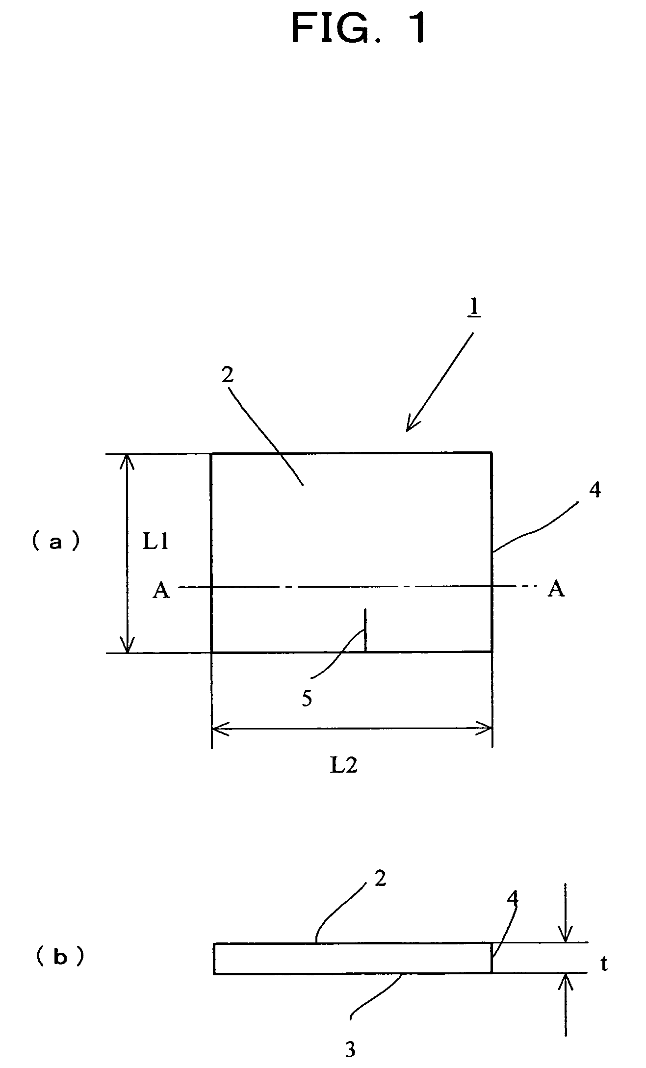
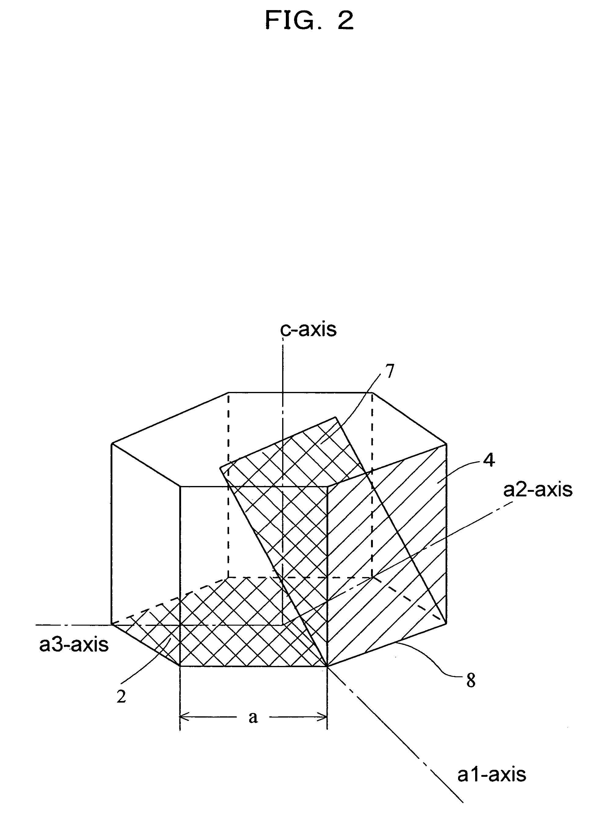
[0047]FIG. 1 has views diagrammatically illustrating the structure of a substrate that represents a first form of implementation of the present invention wherein FIG. 1(a) is a plan view of a diboride XB2 single crystal substrate and FIG. 1(b) is a cross sectional view taken along the line A-A in FIG. 1(a). In FIG. 1, the single crystal substrate, denoted by reference character 1, consists of diboride XB2 (where X is either Zr (zirconium) or Ti (titanium) and B is boron.

[0048]Here, mention is made of the single crystal substrate 1 as being made of ZrB2 when X is Zr as an example. The ZrB2 single crystal substrate 1 has its main surface or front face 2 constituted by a (0001)...


PUM

PropertyMeasurementUnit
thicknessaaaaaaaaaa
thicknessaaaaaaaaaa
thickaaaaaaaaaa

Abstract

Disclosed are a diboride single crystal substrate which has a cleavage plane as same as that of a nitride compound semiconductor and is electrically conductive; a semiconductor laser diode and a semiconductor device using such a substrate and methods of their manufacture wherein the substrate is a single crystal substrate 1 of diboride XB2 (where X is either Zr or Ti) which is facially oriented in a (0001) plane 2 and has a thickness of 0.1 mm or less. The substrate 1 is permitted cleaving and splitting along a (10-10) plane 4 with ease. Using this substrate to form a semiconductor laser diode of a nitride compound, a vertical structure device can be realized. Resonant planes of a semiconductor laser diode with a minimum of loss can be fabricated by splitting the device in a direction parallel to the (10-10) plane. A method of manufacture that eliminates a margin of cutting is also realized.

Description

TECHNICAL FIELD[0001]The present invention relates to a substrate as needed for a nitride compound semiconductor and also to a semiconductor laser diode and more generally a semiconductor device, using such a substrate, and further to a method of making such devices.BACKGROUND ART[0002]Devices such as a semiconductor laser diode (hereinafter referred to as “LD”) and a light emitting diode (hereinafter referred to as “LED”) are applied to a variety of apparatus such as optical disk devices. In recent years, in order to obtain such an optical disk device that is larger in storage capacity, LEDs and LDs are being developed using a nitride compound semiconducting material capable of emitting light in a blue to ultraviolet region that is short in wavelength. A nitride compound semiconductor has a high breakdown voltage owing to it's a large energy band gap. Also, being large in mobility and hence excelling in high frequency properties, a nitride compound semiconductor is being used to de...

Claims


Application Information

Patent Timeline
Patent Type & Authority Patents(United States)
IPC IPC(8): H01L33/00C30B29/10C30B33/00H01L21/20H01L21/331H01L29/04H01L29/24H01L29/737H01L29/93H01L31/0264H01L31/10H01L33/14H01L33/32H01S5/02H01S5/323
CPCC30B29/10C30B33/00H01L21/0242H01L21/02433H01L21/0254H01L29/045H01L29/24H01S5/32341H01L31/0264H01S5/0213H01S5/0218
Inventor OTANI, SHIGEKIKINOSHITA, HIROYUKIMATSUNAMI, HIROYUKISUDA, JUNAMANO, HIROSHIAKASAKI, ISAMUKAMIYAMA, SATOSHI
Owner NAT INST FOR MATERIALS SCI
Why Eureka
Try Eureka