Optical transceiver for computing applications

Active Publication Date: 2008-02-12
SAMTEC
View PDF2 Cites 106 Cited by
  • Summary
  • Abstract
  • Description
  • Claims
  • Application Information

AI Technical Summary

Benefits of technology

[0009]Embodiments of the present invention advantageously decrease the complexity of the manufacturing and reduce the size of the transceiver. By eliminating the transceiver enclosure and using the substrate as a multi-function core element, we reduce the number of components of the transceiver. The substrate acts here as a skeleton. Through elimination of optical pluggability, the transceiver size and form factor are favorably reduced. Furthermore associated with low cost manufacturing technology capable of mass-production, e.g. molding, lamination, wafer processing, and automated pick and place, th

Problems solved by technology

Such high speeds create increasing problems for the technology used for interconnections among the microprocessors, memories, and input/output devices.
For example, copper trace technology, such as conventionally employed on printed circuit boards, is expected to be limited to 15-20 Gigabits per second as a result of signal degradation, power dissipation, and electromagnetic interference unavoidable at such high clock speeds.
Unfortunately all of these potential solutions are costly and power consumptive.
Therefore traditional interconnect scaling will no longer satisfy performance requirements.
Unfortuna

Method used


Image

  • Optical transceiver for computing applications
  • Optical transceiver for computing applications
  • Optical transceiver for computing applications

Examples


Embodiment Construction

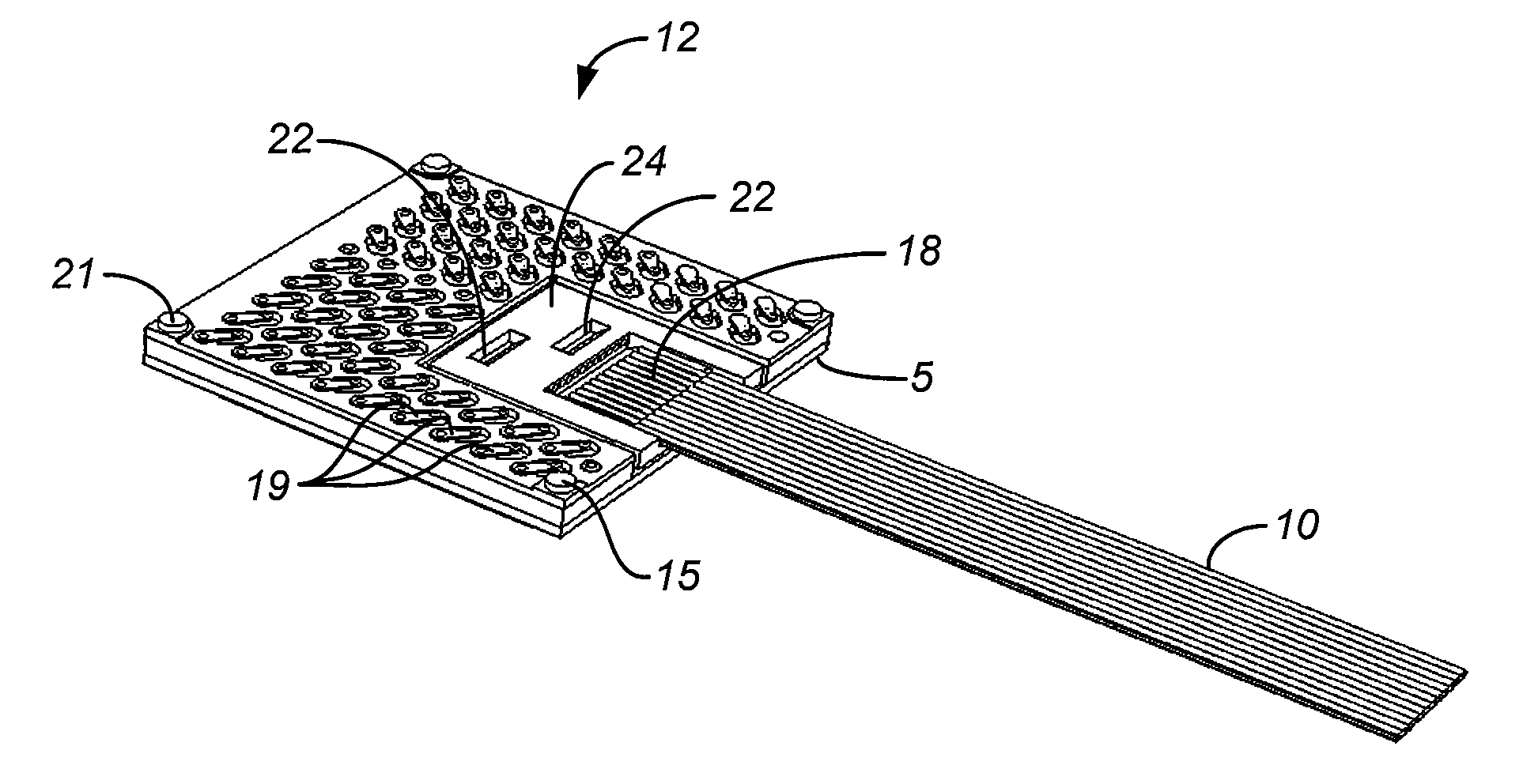
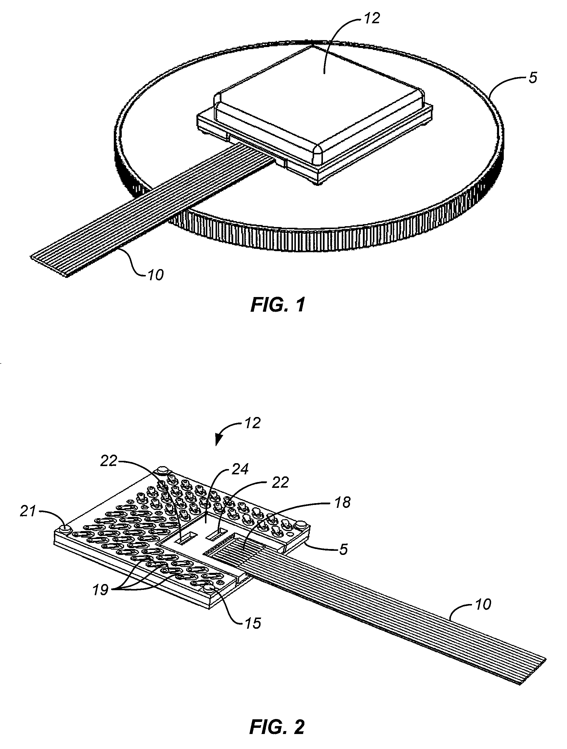
[0026]FIG. 1 is a top view of an optical transceiver according to a preferred embodiment of this invention. The transceiver is depicted on a U.S. quarter dollar coin 5 to illustrate the compact size of the transceiver. The transceiver functions to convert optical signals arriving on optical fibers 10 to electrical signals, and provides them as an output from electrical contacts on the lower surface of the transceiver (not shown in FIG. 1, but see FIG. 2). In addition electrical signals provided to the contacts are converted to optical signals and provided on the optical fibers 10. The device preferably operates as a parallel multimode transceiver with multiple ports, preferably six outputs and six inputs. Of course, different numbers of inputs and outputs, either balanced or unbalanced, can be used. The module 12 illustrated in FIG. 1 includes appropriate electrical terminals, enabling it to be directly mounted on a printed circuit board (PCB), for example, using compliant contacts ...


PUM


Abstract

A compact optical transceiver is provided in which a substrate provides for an alignment surface for optical fibers and a lens assembly provides the necessary optical paths for coupling to laser diode and photodetector structures. Appropriate electrical connections on the substrate enable the substrate to be directly connected to a printed circuit board, grid array socket, and the like.

Description

BACKGROUND OF THE INVENTION[0001]With the continuing growth in performance of computing technology, the interconnect bandwidth required among microprocessors, memories, and input / output devices continues to increase. Such high speeds create increasing problems for the technology used for interconnections among the microprocessors, memories, and input / output devices. For example, copper trace technology, such as conventionally employed on printed circuit boards, is expected to be limited to 15-20 Gigabits per second as a result of signal degradation, power dissipation, and electromagnetic interference unavoidable at such high clock speeds.[0002]Manufacturers of many electronic products have sought to address the limitations of copper by using more exotic substrates with lower dielectric loss or using more sophisticated input / output equalizers at the transmitter and receiver. Unfortunately all of these potential solutions are costly and power consumptive. Therefore traditional interco...

Claims


Application Information

Patent Timeline
IPC IPC(8): G02B6/36
CPCG02B6/4249G02B6/4204G02B6/4214G02B6/4246
Inventor EPITAUX, MARCKIRKPATRICK, PETER E.
Owner SAMTEC
Why Eureka
Try Eureka