Thermophotometric phase shifter and method for fabricating the same

a phase shifter and photometric technology, applied in the direction of optical waveguide light guide, instruments, optics, etc., can solve the problems of deteriorating film quality of polymer, excessive electric power consumption of the entire optical circuit, and inability to meet the requirements of high integration to the thermo-optic parts, so as to improve the strength of the optical waveguide, reduce electric power consumption, and increase the effect of electric power consumption

Inactive Publication Date: 2008-02-19
NEC CORP
View PDF19 Cites 52 Cited by
  • Summary
  • Abstract
  • Description
  • Claims
  • Application Information

AI Technical Summary

Benefits of technology

[0020]Therefore, an object of the present invention is to provide a thermo-optic phase shifter in which a manufacturing process is easy, optical characteristics, mechanical strength, stability and reliability are good, and power consumption is small.

Problems solved by technology

However, when a plurality of thermo-optic phase shifters are provided in one optical circuit for multiple channels, the electric power consumption of the entire optical circuit increases extremely if each thermo-optic phase shifter consumes large electric power.
However, the electric power consumption is still too large for the requirement of high integration to the thermo-optic parts.
However, the above-mentioned conventional techniques have the following problems.
That is, when the optical waveguide is formed of polymer, film quality of the polymer is deteriorated because of the high hygroscopic property of the polymer so that the polymer absorbs the moisture during manufacturing and operation of the thermo-optic phase shifter.
Also, it is difficult to form a passivation protection film on the polymer optical waveguide.
Therefore, the polymer optical waveguide has lower stability and inferiority in reliability, compared with the quartz glass optical waveguides.
However, this method causes various problems such as complication of a manufacturing process, low reproducibility, and increase of propagation loss occurred in an interface of quartz glass and polymer.
However, it is not possible to prevent heat from the heater from being transferred to the substrate.
Thus, the effect to decrease the electric power consumption becomes small.
In addition, in the method of thickening the clad layer under the core layer, there is a problem that a crack generates with a stress generated in the clad layer during the film growth.
Moreover, there is a problem of causing a bend of the substrate with the stress.
Furthermore, an optical characteristic of the optical waveguide is deteriorated because of this stress.
In addition, it is not suitable for mass production because the deposition time becomes long.
Therefore, it is difficult to form the clad layer thick in the process.
The resist layer cannot endure the fluorinated nitric acids and the heater receives damage through the etching.
Thus, there is a problem in the process in the method of the etching of the silicon substrate.
Moreover, the partial removal of the silicon substrate leads to weaken strength of the substrate itself for securing strength of the thermo-optic phase shifter.
Also, the etching of the silicon substrate leads to an unstable state of the optical waveguide since the state of impression of the stress to the clad layer changes.
As a result, mechanical strength and an optical characteristic of the clad layer of the optical waveguide are deteriorated.
105-109), a thermal insulation effect to the optical waveguide is acutely deteriorated because silicon has high thermal conductivity.
Thus, the original purpose of reducing power consumption cannot be accomplished.
Furthermore, in the technique disclosed in Japanese Patent No. 3,152,182, i.e., in which a silicon thin film is provided on the substrate selectively, and a gap is formed between the substrate and the optical waveguide by etching the silicon thin film in a subsequent process, it is a problem that the etching of the silicon thin film is still difficult.
Thus, there is a problem that it is difficult to form the core layer, an over clad layer, and a heater on the under clad layer.

Method used


Image

  • Thermophotometric phase shifter and method for fabricating the same
  • Thermophotometric phase shifter and method for fabricating the same
  • Thermophotometric phase shifter and method for fabricating the same

Examples


first embodiment

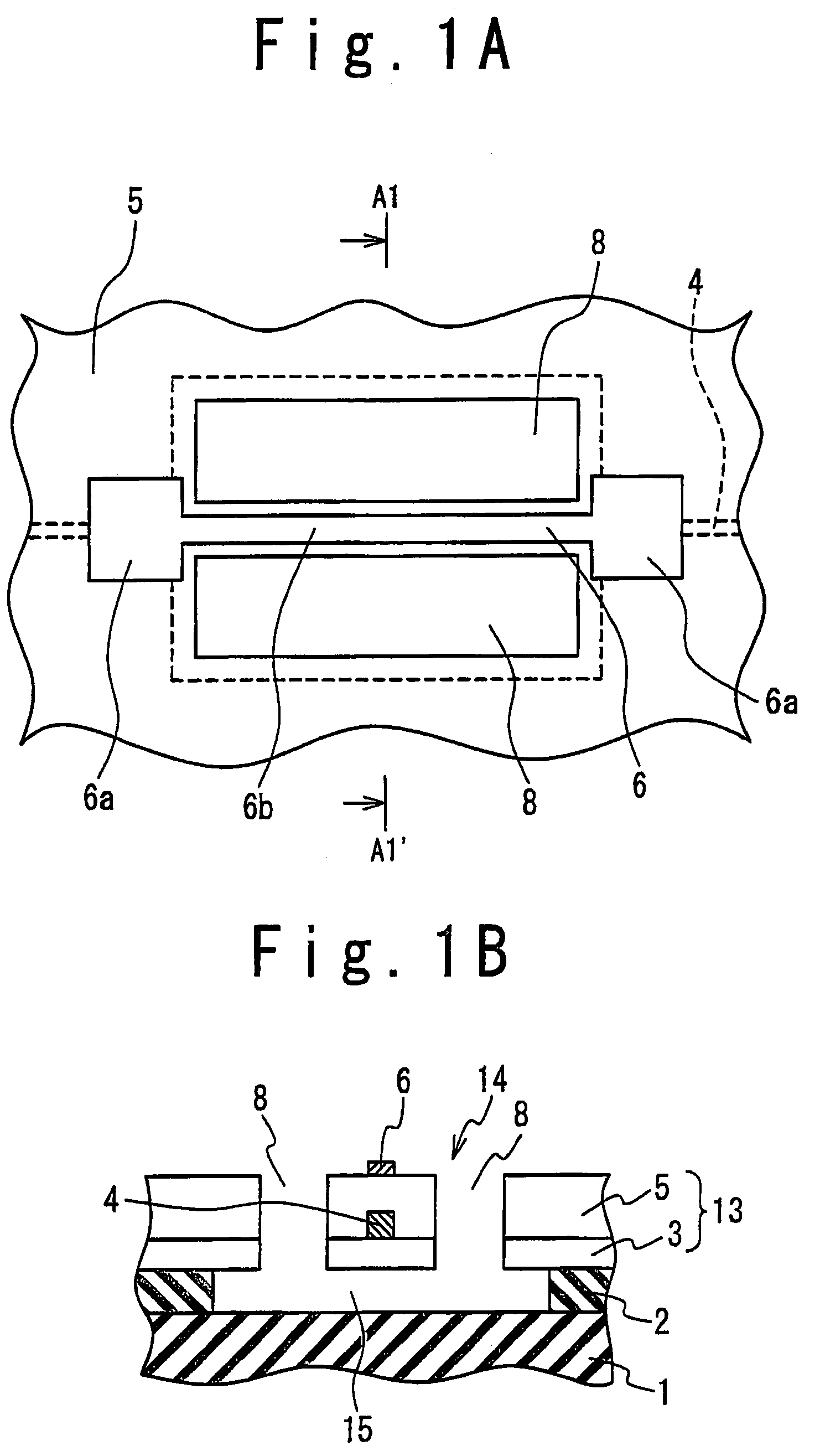
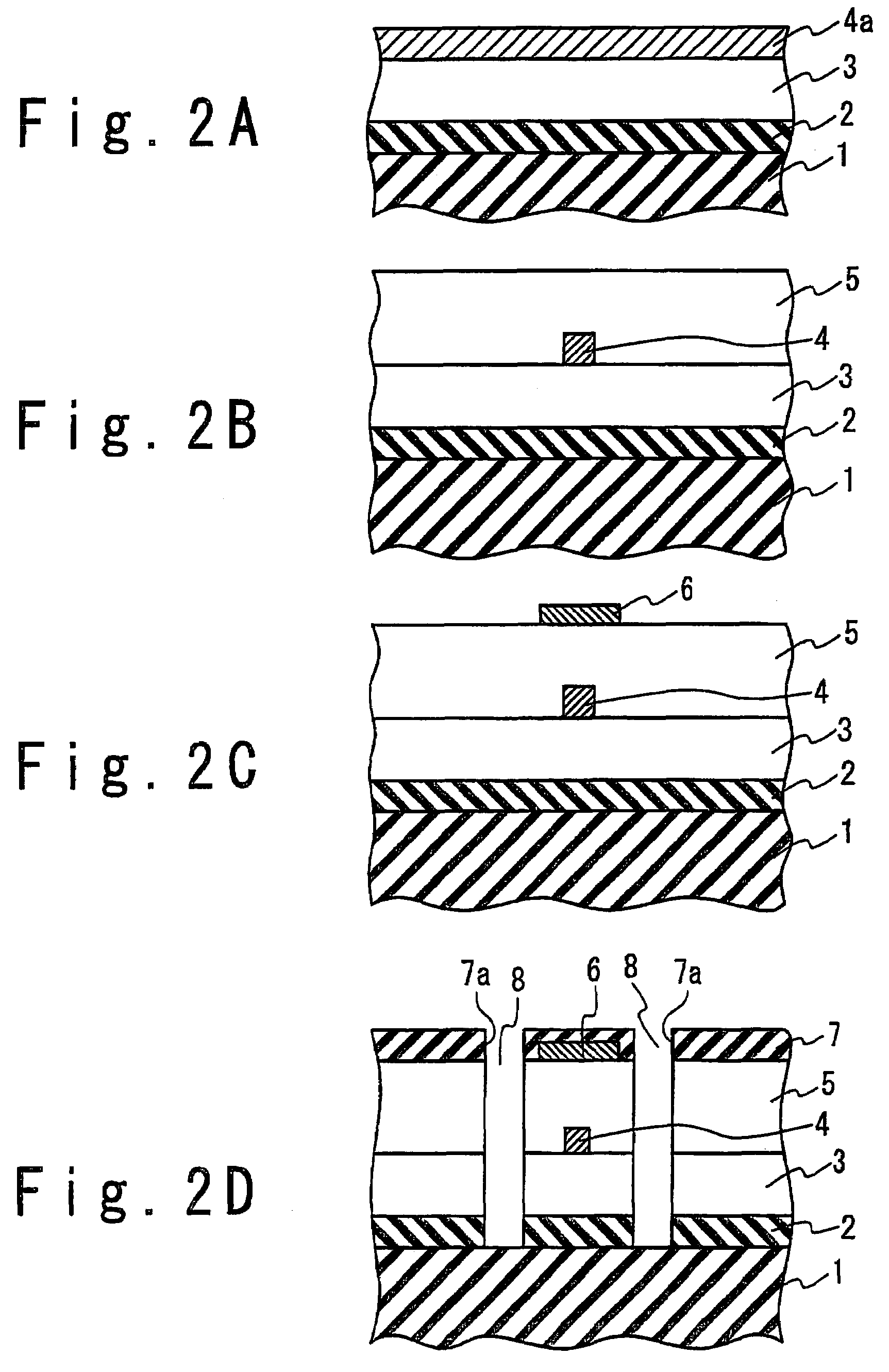
[0093]Next, the method of the manufacturing the thermo-optic phase shifter in the first embodiment will be described. First, as shown in FIG. 2A, the sacrifice layer 2 is formed on the silicon substrate 1 having the thickness of 0.8 mm by an atmosphere pressure chemical vapor deposition method (AP-CVD), for example. The material of the sacrifice layer 2 is sufficient to have a selection etching property to the substrate 1 and the clad layer 13. For instance, the material of the sacrifice layer 2 may be a semiconductor or a glass and the like, and PSG is adopted in the embodiment. Moreover, the film thickness of the sacrifice layer 2 is 5 μm, for instance.

[0094]Next, the glass film having quartz as the main component such as a BPSG film is deposited by the AP-CVD method to have the thickness of 14 μm. Thus, the lower clad layer 3 is formed. A continuous deposition by the AP-CVD method is possible for the PSG of the sacrifice layer 2 and BPSG of the lower clad layer 3 by changing a do...

second embodiment

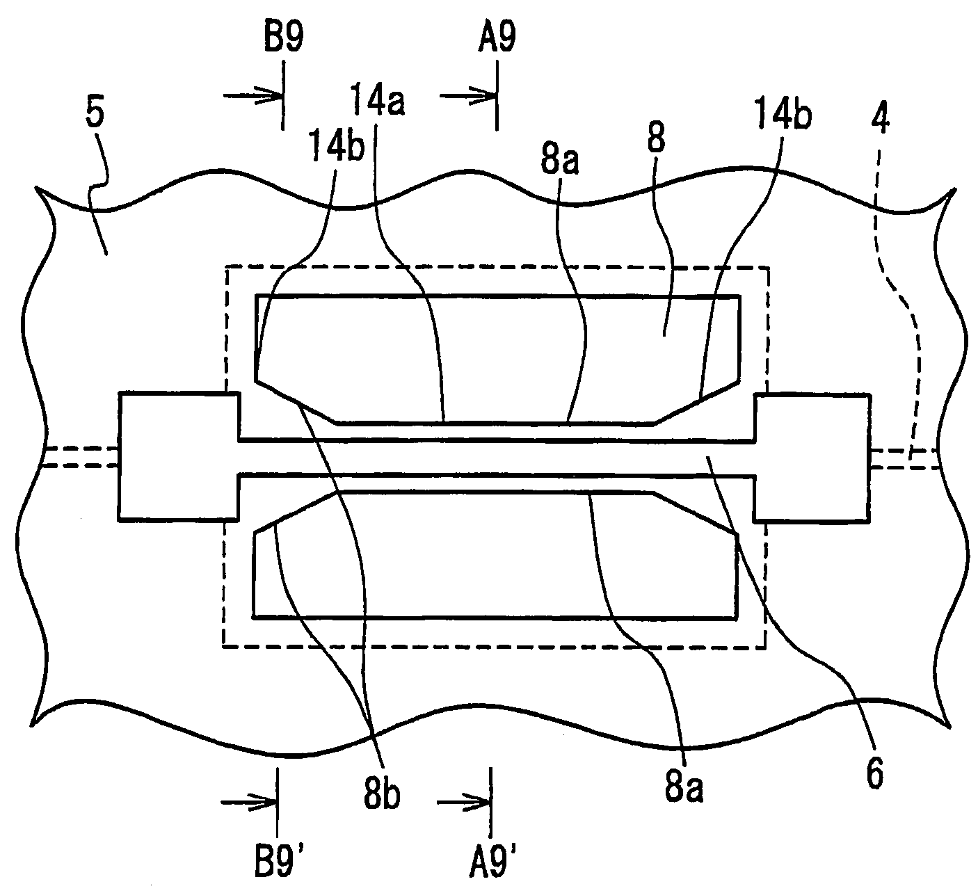
[0110]The electric power consumption of the thermo-optic phase shifter in the second embodiment is greatly dependent on the width of the sacrifice layer 2 to be remained, i.e., the width of the pole 2a. When the light with the wavelength of 1550 nm is inputted to the optical waveguide 14, the electric power consumption necessary to accomplish the phase shift for a half of the wavelength were actually measured. The result is that the electric power consumption is about 60 mW and about 120 mW when the width of the pole 2a is 5 μm and 10 μm, respectively. Therefore, the electric power consumption is decreased enough, comparing with the conventional thermo-optic phase shifter.

[0111]It should be noted that the optical waveguide 14 in the second embodiment needs 6 to 12 times of the electric power of the optical waveguide in the first embodiment which is completely separated from the substrate. However, the mechanical strength of the thermo-optic phase shifter in the second embodiment is ...

third embodiment

[0117]In the third embodiment, the sacrifice layer is selectively etched and one process is added. However, the stress generated in the sacrifice layer can be released. Therefore, the polarization dependence of the optical waveguide 14 can be decreased further more, and the optical characteristic can be improved more. Since the patterning of the sacrifice layer 2 is previously carried out, etching variation when the sacrifice layer 2 is removed by the wet etching can be resolved, then further reliability and the improvement of yield can be accomplished.

[0118]In addition, BHF can be used as etchant by forming the sacrifice layer 2 of PSG. Therefore, it is not needed that the sacrifice layer is formed of silicon and the fluorinated nitric acid is used as etchant, as disclosed in the above-mentioned Japanese Patent No. 3,152,182. Therefore, the thermo-optic phase shifter in the third embodiment is easier in manufacture than the thermo-optic phase shifter disclosed in the patent No. 3,1...


PUM

PropertyMeasurementUnit
lengthaaaaaaaaaa
distanceaaaaaaaaaa
thicknessaaaaaaaaaa

Abstract

In an aspect of the present invention, a thermo-optic phase shifter includes a substrate, a heater, a clad layer formed directly or indirectly on a substrate, an optical waveguide clad layer formed apart from the substrate and the clad layer in a portion corresponding to the heater, and a core layer provided inside said bridge section clad layer. The optical waveguide clad layer is connected with the clad layer in a portion of the phase shifter other than the heater corresponding portion. The optical waveguide clad layer and the core layer form an optical waveguide in the heater corresponding portion. The heater is provided inside or outside the optical waveguide apart from the core layer in the heater corresponding portion, and generates heat to change a phase of a light signal propagated in the optical waveguide.

Description

TECHNICAL FIELD[0001]The present invention relates to a thermo-optic phase shifter with electric power consumption reduced and a manufacturing method of the same.BACKGROUND ART[0002]In an optical communication field, a multi channel communication is rapidly promoted by the advent of a WDM (wavelength division multiplexing) communication system. In accompaniment by this, optical elements of a number corresponding to the number of channels are needed in order to achieve a functional control of each channel, for instance, controlling power of each channel to a constant power and controlling of switching.[0003]For this reason, small-sized optical circuit parts are highly needed that can be applied to optical switches and enables a high-density integration. A light switch of a single unit has already been practiced. A matrix switch has been practiced in which the large number of these light switches is used and which has a plurality input-output ports. Various techniques are proposed to ...

Claims


Application Information

Patent Timeline
Patent Type & Authority Patents(United States)
IPC IPC(8): G02F1/01G02B6/12G02B6/13
CPCG02F1/011G02F1/0147G02F2203/50
Inventor TAKAHASHI, MORIO
Owner NEC CORP
Why Eureka
Try Eureka