
Semiconductor memory

a technology of memory and semiconductors, applied in thermoelectric devices, bulk negative resistance effect devices, instruments, etc., can solve the problems of information loss, information stored in capacitors must be renewed, information loss is also caused, etc., and achieves short switching times and low programming voltages.

Inactive Publication Date: 2008-03-18
POLARIS INNOVATIONS LTD
View PDF9 Cites 4 Cited by
  • Summary
  • Abstract
  • Description
  • Claims
  • Application Information

AI Technical Summary

Benefits of technology

"The present invention provides a non-volatile semiconductor memory that has good scalability and low switching times. It uses a memory cell with a matrix of open or disturbed nanocrystalline or amorphous network structures with structural voids. The memory cell is connected at the crosspoints of electric supply lines, and the matrix material has a resistively switching property between two stable states that is caused by the movement of ions. The memory cell is in a high-resistance state when there is no electric field, and it can be switched to a low-resistance state by applying a negative voltage pulse. The memory cell is compatible with CMOS process technology and has a controllable pore size and density. The memory mechanism is based on the mobility of ions in a chemically inert, high-resistance matrix."

Problems solved by technology

In real systems of non-volatile memory devices, the stored charge, however, will not remain in the capacitor for any long time, which may result in a loss of information.
On the other hand, the loss of information is also caused by so-called leaking paths that are generated during the manufacturing or processing of the memory devices, e.g. unsaturated bonds at interfaces between different materials as well as differing structure dimensions due to process fluctuations.
In both cases, these leaking paths result in that the information stored in the capacitor has to be renewed in time before it is lost.
The problem of the leaking currents in the memory capacitor existing with the DRAM memory concept, which results in a loss of charge, has so far been solved insufficiently only by the permanent refreshing of the stored charge.
The flash memory concept underlies the problem of limited write and read cycles with barrier layers, wherein no optimum solution has been found yet for the high voltages and the slow read and write cycles.
Furthermore, the above-mentioned memory concepts (charge trapping, flash and DRAM memories) will, due to their functioning that is based on the storing of charges, presumably meet with physical scaling limits within foreseeable time.
Furthermore, in the case of the flash memory concept, the high switching voltages and the limited number of read and write cycles, and in the case of the DRAM memory concept the limited duration of the storage of the charge state constitute additional problems that have not been solved optimally so far.

Method used


Image

  • Semiconductor memory
  • Semiconductor memory

Examples


first embodiment

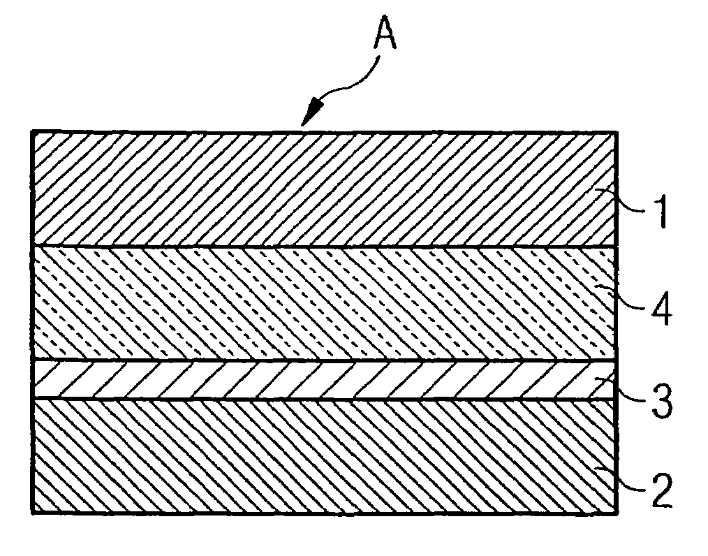
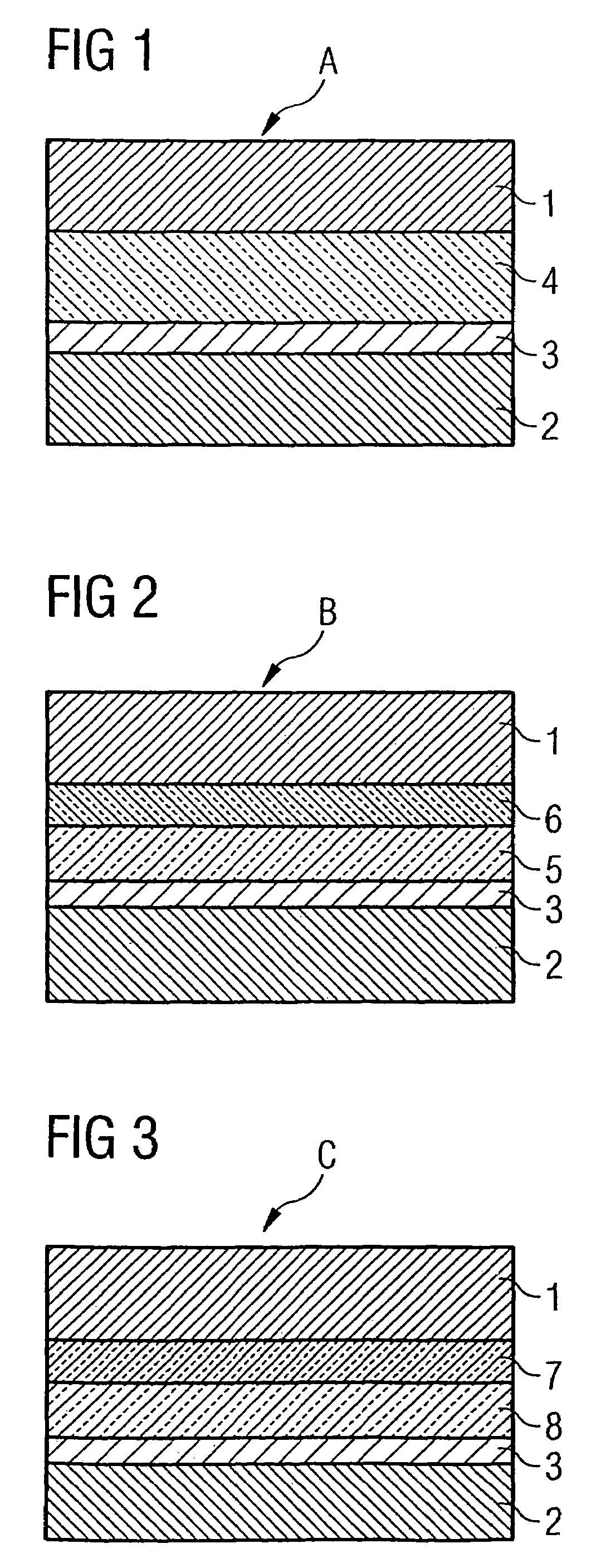
[0033]The amorphous, micromorphous or microcrystalline silicon material 4 used in the first embodiment preferably comprises one of the following compounds: amorphous Si:H, amorphous Si:C,H, amorphous Si:H,O, μc-Si, or SiOx (x=1 . . . 2), wherein other (foreign) components may also be added as alloys, e.g. amorphous Ge:H or materials derived therefrom.

[0034]FIG. 2 shows the schematic layer structure of a second preferred embodiment of the inventive non-volatile memory cell B that has a resistively switching property on the basis of ion drift. According to this second preferred embodiment, the resistively switching, non-volatile memory cell comprises—instead of the amorphous, micromorphous or microcrystalline silicon matrix material layer 4 doped with alkali, earth alkali or metal ions—a double layer 5, 6 with a strongly ion-doped silicon layer 5 and a silicon layer 6 that is non-doped with respect to highly movable alkali, earth alkali and metal ions.

[0035]Consequently, the resistive...

third embodiment

[0048]Alternatively, in this third embodiment, the double layer 7, 8 may also be designed as a single silicon layer comprising a doping profile that proceeds from strong doping to weak doping.

[0049]The inventive memory cell A, B, C is preferably manufactured by a CMOS process-compatible method. The layer arrangements described above may optionally be realized in horizontal or in vertical design on a semiconductor substrate and are independent both of the selected electrode materials and of the choice of an amorphous, micromorphous or microcrystalline silicon diffusion matrix. Electrode materials that generate an ohmic contact to amorphous Si-layers have already been known. The electrode materials are preferably manufactured of inert or refractory elements such as W, Mo, or Ti, which establish a good ohmic contact to the silicon matrix materials doped with highly movable ions.

[0050]According to a further aspect of the present invention, there is a method for manufacturing a resistive...


PUM


Abstract

The object of providing a non-volatile semiconductor memory that stands out by good scalability and a high retention time as well as ensures low switching voltages at low switching times and achieves a great number of switching cycles at good temperature stability is solved by the present invention with a semiconductor memory whose memory cells comprise at least one silicon matrix material layer with open or disturbed nanocrystalline or amorphous network structures and structural voids which has a resistively switching property between two stable states, utilizing the ion drift in the silicon matrix material layer. The memory concept suggested in the present invention thus offers an alternative to the flash and DRAM memory concepts since it is not based on the storing of charges, but on the difference of the electric resistance between two stable states that are caused by the mobility of ions in the amorphous silicon matrix material with an externally applied electric field.

Description

CLAIM FOR PRIORITY[0001]This application claims priority to German Application No. 10 2004 046 391.1, filed Sep. 24, 2004, which is incorporated herein, in its entirety, by reference.TECHNICAL FIELD OF THE INVENTION[0002]The invention relates to a semiconductor memory, in particular a non-volatile semiconductor memory with resistively switching memory cells. The invention further relates to a method for manufacturing a non-volatile, resistively switching memory cell.BACKGROUND OF THE INVENTION[0003]In a semiconductor memory device, a cell field consisting of a plurality of memory cells and a matrix of column and row supply lines or word and bit lines, respectively, is usually built up. These supply lines consist of electrically conducting material, with the actual memory cell being positioned at the crosspoints of the supply lines. To perform a change of the information content in a particular memory cell at the addressed crosspoint or to recall the content of the memory cell, the c...

Claims


Application Information

Patent Timeline
Patent Type & Authority Patents(United States)
IPC IPC(8): H01L47/00H01L35/24H01L51/00H10N80/00H10N10/856
CPCG11C13/0009G11C13/0069H01L45/1658H01L45/085H01L45/1233H01L45/148H01L45/1616G11C2013/009G11C2213/11G11C2213/33G11C2213/55G11C2213/77G11C2213/56H10N70/245H10N70/884H10N70/826H10N70/023H10N70/046
Inventor UFERT, KLAUS-DIETER
Owner POLARIS INNOVATIONS LTD
Learn More