N/PMOS saturation current, HCE, and Vt stability by contact etch stop film modifications
a technology of contact etching and stop film, which is applied in the direction of basic electric elements, electrical apparatus, and semiconductor devices, can solve the problems of significant deformation of hot carrier lifetime and vt stability, change of threshold voltage (vt), and reducing the reliability of mosfet, so as to reduce the hydrogen content in the nitride layer
- Summary
- Abstract
- Description
- Claims
- Application Information
AI Technical Summary
Benefits of technology
Problems solved by technology
Method used
Image
Examples
first embodiment
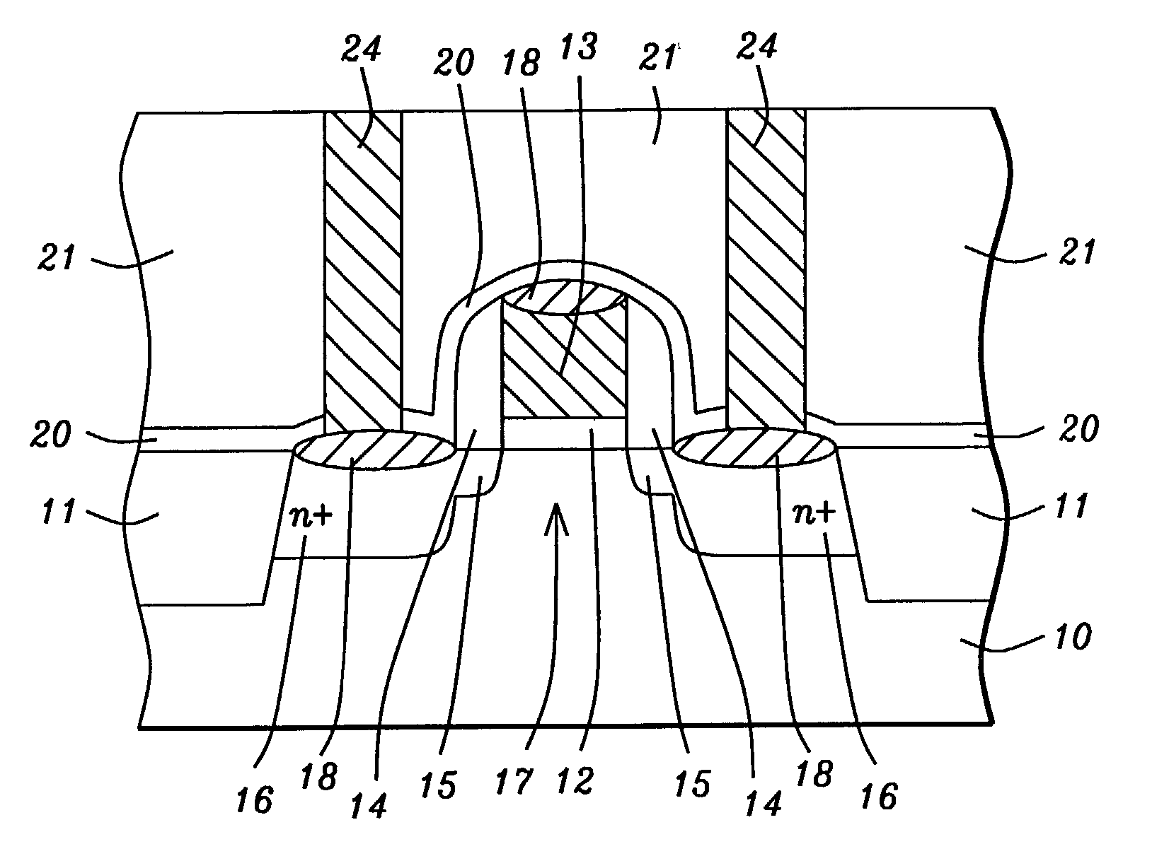
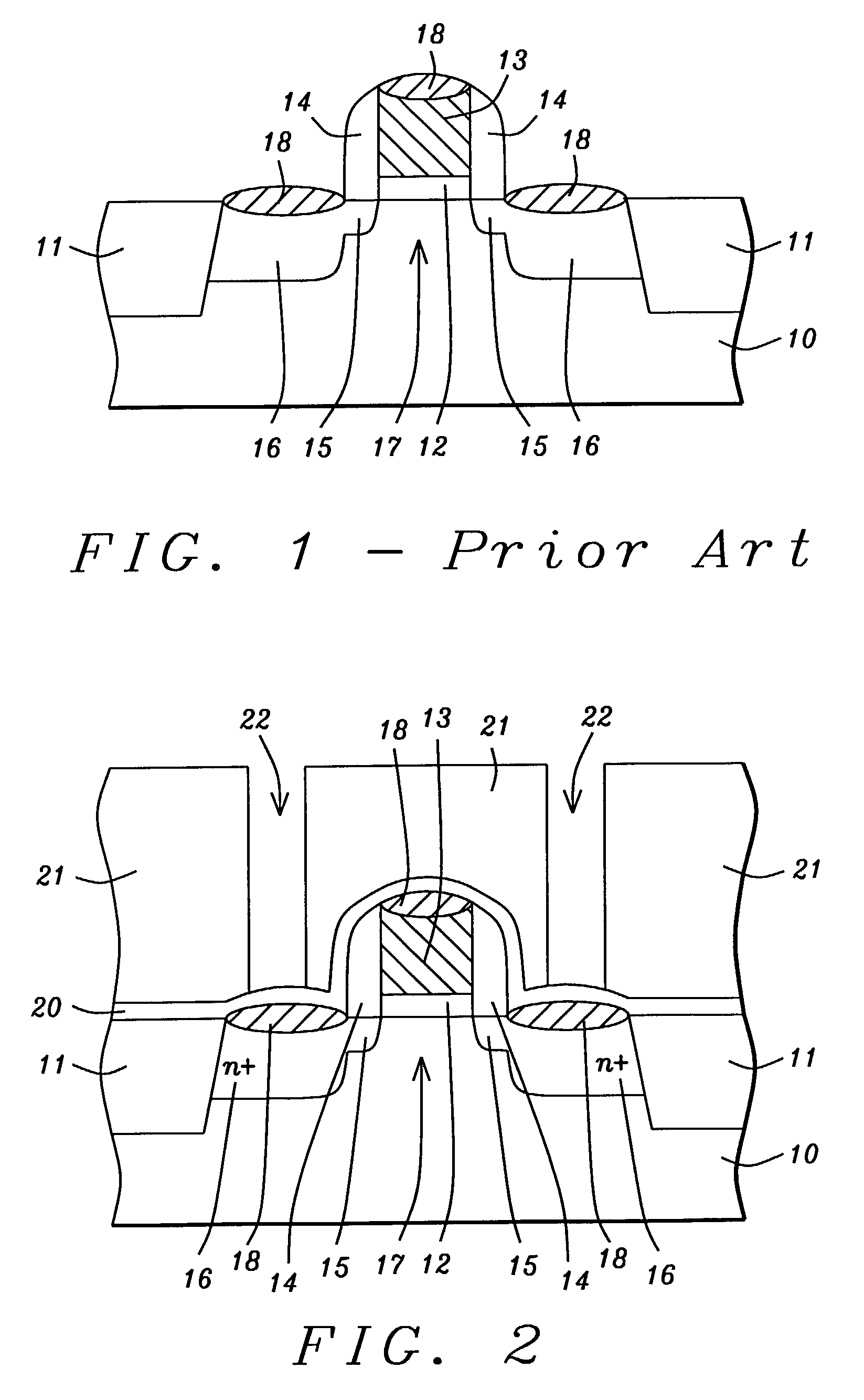
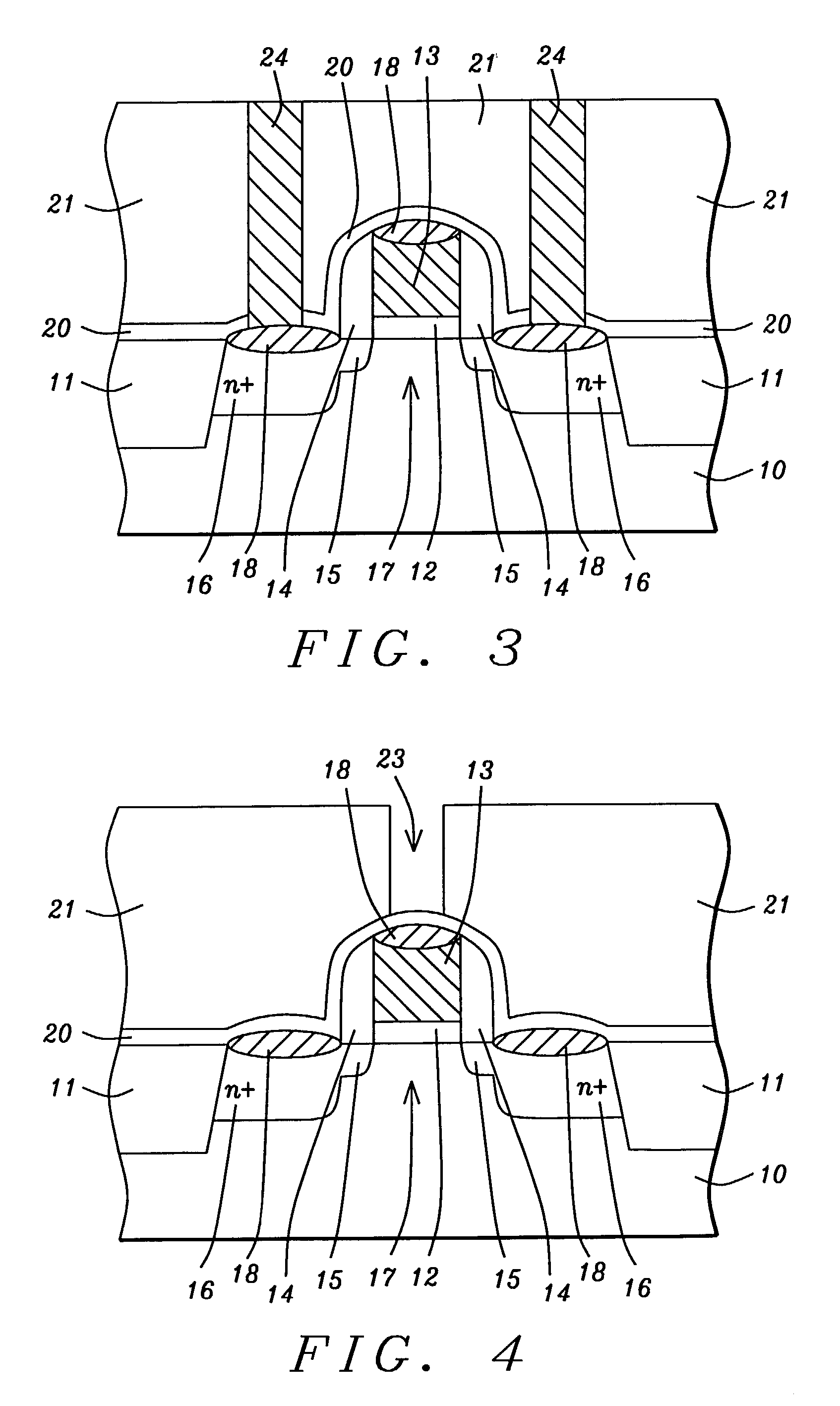
[0021]The first embodiment is illustrated in FIGS. 2-5. Referring to FIG. 2, a substrate 10 is provided that is typically silicon and is comprised of active and passive devices in a substructure (not shown). An NMOS transistor is fabricated by conventional means between shallow trench isolation (STI) features 11 that are filled with a dielectric material such as SiO2. The NMOS transistor is comprised of a gate dielectric layer 12 such as SiO2, a gate electrode 13 which is normally polysilicon or amorphous silicon, sidewall spacers 14, lightly doped source / drain regions 15, heavily doped source / drain regions 16, channel 17, and silicide regions 18.
[0022]The NMOS transistor is further defined according to the present invention by forming a conformal etch stop layer 20 on STI regions 11, silicide regions 18, and on sidewall spacers 14. Etch stop layer 20 is preferably comprised of silicon nitride that is deposited to a thickness of between 200 and 600 Angstroms by a plasma enhanced che...
second embodiment
[0030]A second embodiment is illustrated in FIGS. 6-9. Referring to FIG. 6, a substrate 30 is provided that is typically silicon and is comprised of active and passive devices in a substructure (not shown). A PMOS transistor is fabricated by conventional means between shallow trench isolation (STI) features 31 that are filled with a dielectric material such as SiO2. The PMOS transistor is comprised of a gate dielectric layer 32 such as SiO2, a gate electrode 33 that is normally polysilicon or amorphous silicon, sidewall spacers 34, lightly doped source / drain regions 35, heavily doped source / drain regions 36, channel 37, and silicide regions 38.
[0031]The PMOS transistor is further defined according to the present invention by forming a conformal etch stop layer 40 on STI regions 31, silicide regions 38, and on spacers 34. Etch stop layer 40 is preferably comprised of silicon nitride that is deposited to a thickness of between 200 and 600 Angstroms by a PECVD technique. The process co...
PUM
 Abstract
Description
Claims
Application Information


