Resin encapsulated semiconductor device and the production method

a technology of encapsulation and semiconductors, applied in the direction of printed circuit manufacturing, printed circuit components, printed circuit assembling, etc., can solve the problems of failure of an entire system, material fracture, crack generation, etc., and achieve superior thermal radiation characteristics and strength reliability, superior strength characteristics, and reduced stress fatigue

Active Publication Date: 2008-05-13
HITACHI LTD +1
View PDF15 Cites 7 Cited by
  • Summary
  • Abstract
  • Description
  • Claims
  • Application Information

AI Technical Summary

Benefits of technology

[0014]It is an object of the present invention to provide a resin encapsulated semiconductor module device having both high strength and high thermal conductivity such that it can be applied to fields where various types of strict reliabilities, such as for mounting on automobiles, are required, and to provide a manufacturing method thereof.
[0019]The maximum diameter of the metal particles or the maximum height of the metal protrusions is in a range of 50 μm to 200 μm. The amount of the elements added is in a range of 0.005 vol % to 5 vol % relative to the volume of conductive component in the bonding material. This prevents aggregation and a path can be readily formed.
[0021]The conditions of the reduced pressure comprise a condition such that a void generated in the first bonding material in the reflow step is removed from the end of the board, thereby readily moving a gas in the first bonding material.
[0022]According to the present invention, by using a circuit board in which thick metal plates are bonded to both sides of silicon nitride that is superior in strength characteristics and by soldering the circuit board to a solder layer mounted on a base plate with substantially spherical elements disposed on the solder layer under reduced pressure, almost no void-like defects are generated in the solder layer, thereby realizing a semiconductor device superior in thermal radiation characteristics and strength reliability as compared with a semiconductor device in which a conventional circuit board is used.
[0023]Also, by employing the circuit board in which thick metal plates are bonded to both sides of silicon nitride, it becomes possible to approximate the thermal expansion coefficient of the circuit board to the thermal expansion coefficient of a metal base plate, thereby reducing stress fatigue generated in a solder portion that bonds the circuit board and the metal base plate and realizing a longer operating life for the semiconductor device.

Problems solved by technology

However, aluminum nitride is somewhat inferior in terms of strength characteristics.
When thermal strain is repeatedly provided as in a heat cycle, or vibration or shock is repeatedly provided, the generation of material fracture, such as cracking, is problematic.
If a circuit board is configured using a material subject to material fracture as an insulated layer, the aforementioned material fracture may lead to the failure of an entire system resulting from the insulated fracture of the circuit board, the impediment of a thermal path in a mounted member having high thermal radiation, or the like.
However, in practical applications, it is difficult to realize high strength and high thermal conductivity.

Method used


Image

  • Resin encapsulated semiconductor device and the production method
  • Resin encapsulated semiconductor device and the production method
  • Resin encapsulated semiconductor device and the production method

Examples


Embodiment Construction

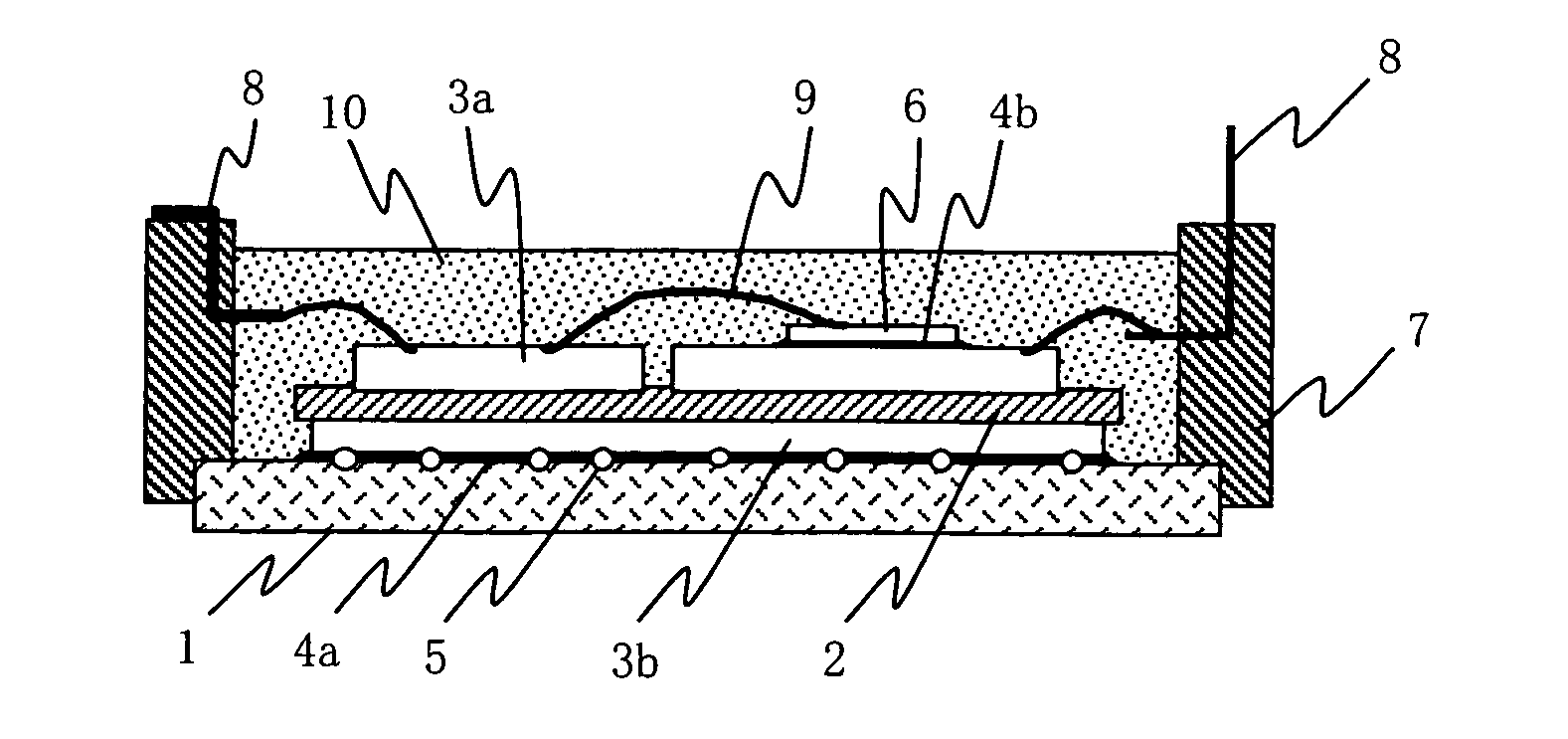
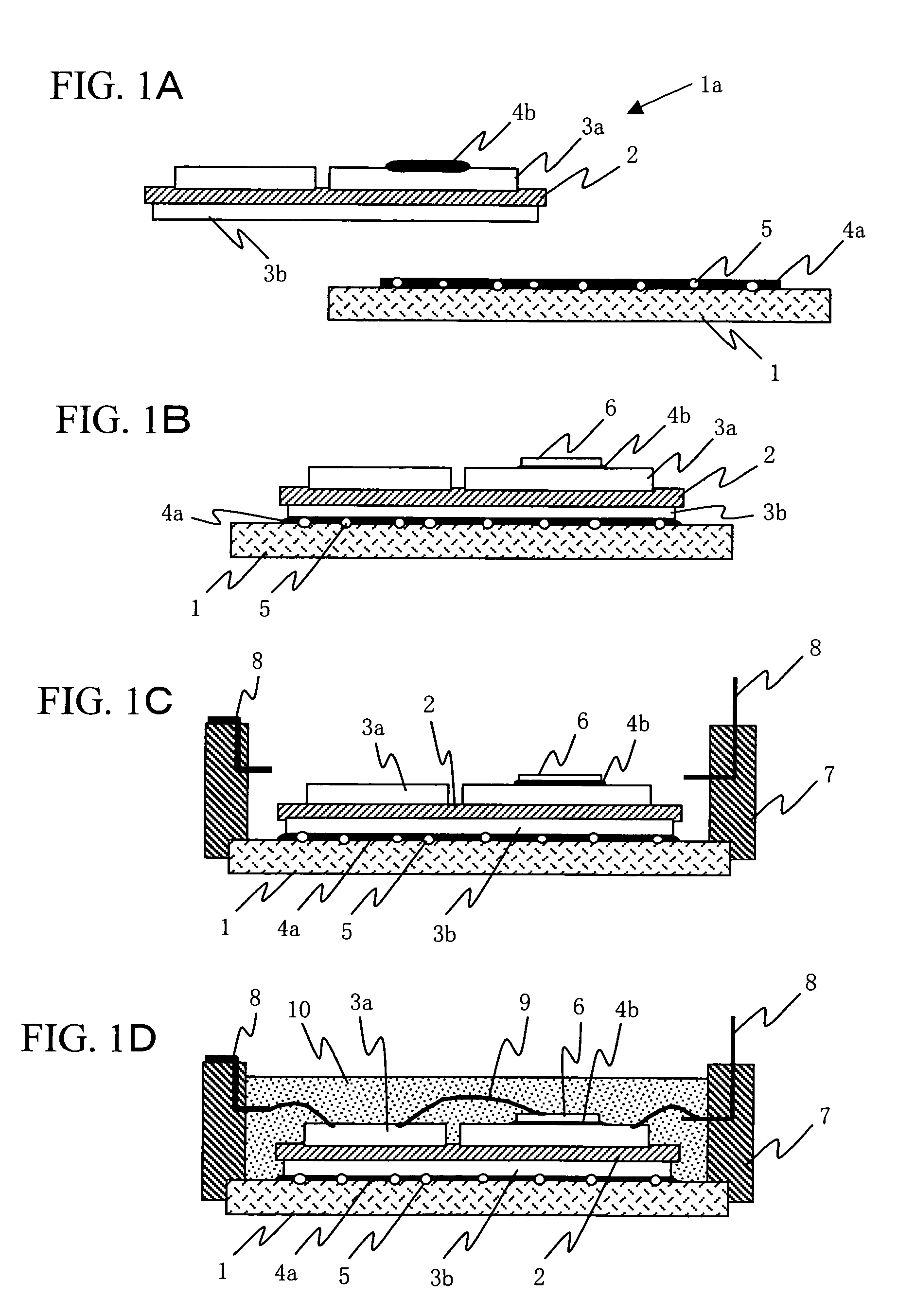
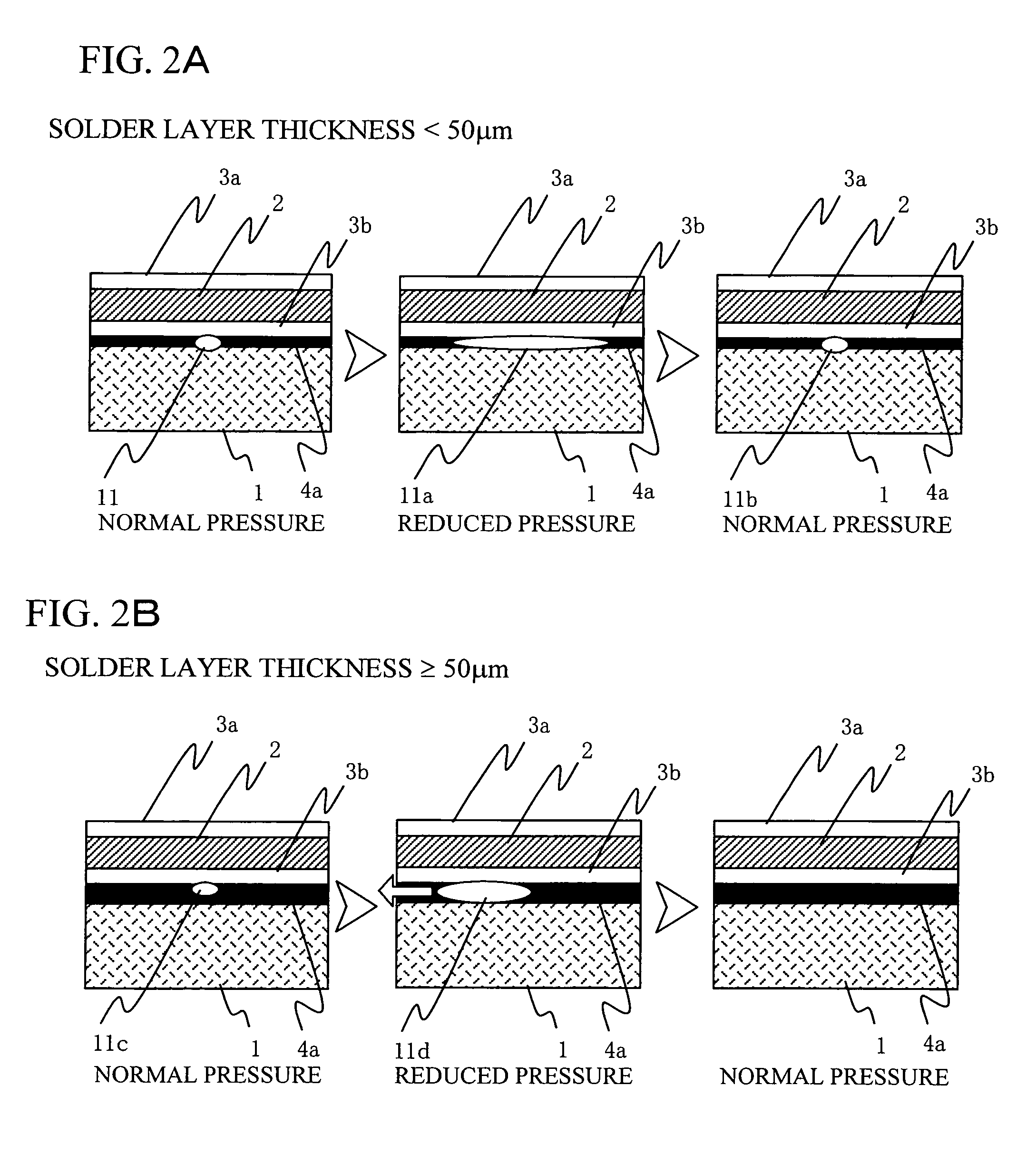
[0029]When silicon nitride inferior to aluminum nitride in thermal conductivity is used as the insulated layer of the circuit board, if the thickness of the insulated layer is reduced in a range by which insulated characteristics can be secured, it becomes possible to approximate the thermal radiation characteristics to those of an aluminum nitride circuit board. Further, if the thickness of metal plates bonded to both sides of the insulated layer is increased to improve thermal spread, it becomes possible to realize a circuit board superior in thermal conductivity than in the case where aluminum nitride is used. By bonding thick metal plates to a thin insulated layer, defects, such as cracking, are likely to be generated in the insulated layer due to stress generated upon soldering. However, the aforementioned configuration can be realized by using silicon nitride superior in strength characteristics.

[0030]However, when the circuit board is mounted on a base plate of good thermal c...


PUM

PropertyMeasurementUnit
thicknessaaaaaaaaaa
thicknessaaaaaaaaaa
thicknessaaaaaaaaaa

Abstract

A semiconductor device having both high strength and high thermal radiation that is capable of being applied to mounting on automobiles experiencing many thermal cycles, and a manufacturing method thereof are provided. A circuit board 1a for a resin encapsulated semiconductor module device has a configuration where a silicon nitride plate 2 with a thickness of 0.635 mm has copper plates of 1.0 mm and 0.8 mm bonded to both sides thereof via active metal. A copper plate 3a is bonded to the surface side of the silicon nitride plate 2, and a prescribed circuit pattern is formed on the copper plate 3a. Tin-silver-copper cream solder layers 4a and 4b with a thickness of 200 μm are formed at a prescribed location on the circuit pattern 3a on which a semiconductor element 6 is mounted and at a prescribed location of a base plate 1 on which the circuit board 1a is disposed. Nickel particles 5 having a maximum particle size of 100 μm and an average particle size of 70 μm are dispersed in the solder 4a on the base plate 1 of good thermal conductivity. A semiconductor element (chip) 6, the circuit board 1a, and the base plate 1 are disposed on predetermined locations. Thereafter, they are set in a reflow oven (not shown in the drawings) for reflow soldering. After the inside of the reflow oven is replaced by a nitrogen atmosphere, the reflow oven is heated to 280° C. At the time when solder is melted, the inside of the oven is decompressed to 1 Pa, nitrogen is introduced, and the reflow oven is cooled to about room temperature, thereby completing the solder bonding step. After flux is washed, an outer case 7 with an insert-molded outlet terminal 8 is adhered to the base plate 1 and a predetermined connection is conducted via an aluminum bonding wire 9. Then, silicone gel 10 is injected into a package delimited via the base plate 1 and the outer case 7, and the silicone gel 10 is heat-hardened, thereby completing a resin encapsulated semiconductor device A.

Description

[0001]This application is based on the Japanese Patent Application JP2004-073305, filed on Mar. 15, 2004, all the contents of witch is incorporated in this application by reference.BACKGROUND OF THE INVENTION[0002]1. Field of the Invention[0003]The present invention relates to a power semiconductor module device, especially to a resin encapsulated power semiconductor module device that realizes effective thermal radiation, and a production method thereof.[0004]2. Background Art[0005]Conventionally, power semiconductor module devices have been used for electronic devices such as inverters, converters, servos, and the like. FIG. 5 shows a cross-sectional view of a conventional power semiconductor module device. As shown in FIG. 5, the power semiconductor module device comprises a circuit board with metal plates 103a and 103b bonded to both sides of a ceramic material 102, the circuit board being fixed on a metal base plate 101 using solder 104a. And a semiconductor element 106 is fixe...

Claims


Application Information

Patent Timeline
Patent Type & Authority Patents(United States)
IPC IPC(8): H01L23/34H01L23/12H01L21/44H01L21/58H01L23/24H01L23/36H01L23/373H01L23/488H01L23/498H01L25/07H01L25/18H01R43/02H05K1/03H05K3/00H05K3/34
CPCH01L23/24H01L23/3735H05K3/0061H01L23/488H01L2924/1305H01L2924/01028H01L2924/01013H01L2924/01019H01L24/48H05K2201/2036H05K2201/0215H05K3/341H05K1/0306H01L2924/19107H01L2924/13091H01L2924/13055H01L2924/01079H01L24/45H01L2224/32225H01L2224/45124H01L2224/48091H01L2224/48227H01L2224/73265H01L2224/92247H01L2924/01014H01L2924/0105H01L2924/01078H01L2924/00014H01L2924/00012H01L2924/00H01L24/73H01L2924/181
Inventor SUZUKI, KAZUHIROMORITA, TOSHIAKIIMAMURA, HISAYUKIWATANABE, JUNICHICHIBA, MITSUAKI
Owner HITACHI LTD
Why Eureka
Try Eureka