Method for crystallizing amorphous semiconductor thin film by epitaxial growth using non-metal seed and method for fabricating poly-crystalline thin film transistor using the same

a technology of amorphous semiconductors and epitaxial growth, which is applied in the direction of crystal growth process, polycrystalline material growth, chemistry apparatus and processes, etc., can solve the problems of deteriorating electrical characteristics of thin film transistors, surface roughness and crystallization uniformity, and fundamental problems that have not been solved, so as to remove the source of metal pollution and improve the characteristics of semiconductor devices

Inactive Publication Date: 2008-06-24
PAIK WOON SUH
View PDF9 Cites 14 Cited by
  • Summary
  • Abstract
  • Description
  • Claims
  • Application Information

AI Technical Summary

Benefits of technology

[0021]To solve the above problems, it is an object of the present invention to provide a method of crystallizing an amorphous semiconductor thin film which can manufacture a thin film transistor of excellent features by a non-metal seed epitaxial growth (NSEG) method, in which a poly-crystalline semiconductor thin film is epitaxially grown using crystallization induced non-metal seeds which are buried below the amorphous semiconductor thin film, at a low temperature of 600° C. or lower at which a glass substrate can tolerate, to thereby realize crystallization of the amorphous semiconductor thin film having no metal pollution.
[0022]It is another object of the present invention to provide a method of crystallizing an amorphous semiconductor thin film and a method of fabricating a poly-crystalline semiconductor thin film transistor using the same, in which a heat-treatment time necessary for crystallizing an amorphous semiconductor thin film can be reduced using crystallization induced non-metal seeds buried below the amorphous semiconductor thin film and crystallization induced metal formed on the upper surface of the amorphous semiconductor thin film, and a lightly doped drain (LDD) structure can be formed without having an ion-injection process by applying an off-set structure at the time of forming a pattern of the crystallization induced metal.
[0023]It is still another object of the present invention to provide a method of crystallizing an amorphous semiconductor thin film which prevents an interface characteristic from worsening between a semiconductor layer and a gate insulation film due to reduction in volume of silicon at the time of crystallizing of the amorphous silicon and can reduce a total of heat treatment time, by crystallizing the entire semiconductor layer at the time of a primary heat treatment before impurities are doped and activating the injected impurities at the time of a secondary heat treatment after the impurities have been doped, when a poly-crystalline semiconductor thin film is epitaxially grown by a non-metal seed epitaxial growth (NSEG) method.
[0024]It is yet another object of the present invention to provide a method of fabricating a low-temperature poly-crystalline thin film transistor having excellent electrical characteristics, which is fabricated using a crystallized semiconductor thin film obtained by using non-metal seeds.
[0036]As described above, in the case that the amorphous silicon is crystallized at a low temperature by a non-metal seed epitaxial growth (NSEG) method according to the present invention, silicide is formed before crystallization heat-treatment is performed, and the remaining metal is removed, to thereby remove the source of metal pollution in the silicon and thus improve characteristics of a semiconductor device.

Problems solved by technology

The eximer laser annealing (ELA) method requires for expansive equipment and crystallize silicon by a scanning process, and thus has defects in view of surface roughness and crystallization uniformity.
However, since the MILC method uses crystallization induced metal, electrical characteristics of a thin film transistor deteriorate due to metal pollution.
Although various methods have been developed in order to suppress them, fundamental problems have not been solved yet.
As described above, the conventional crystallization method using a conventional laser heat treatment process requires for expansive equipment and has non-uniform crystallization and inferior surface roughness.
As a result, a production cost becomes high and a yield is lowered.
Also, metal pollution occurring on a metal film deposited on the amorphous silicon surface for the conventional MILC method exists in the poly-crystalline silicon film, to thus deteriorate an electrical feature of a device (see IEEE Trans.

Method used


Image

  • Method for crystallizing amorphous semiconductor thin film by epitaxial growth using non-metal seed and method for fabricating poly-crystalline thin film transistor using the same
  • Method for crystallizing amorphous semiconductor thin film by epitaxial growth using non-metal seed and method for fabricating poly-crystalline thin film transistor using the same
  • Method for crystallizing amorphous semiconductor thin film by epitaxial growth using non-metal seed and method for fabricating poly-crystalline thin film transistor using the same

Examples


first embodiment

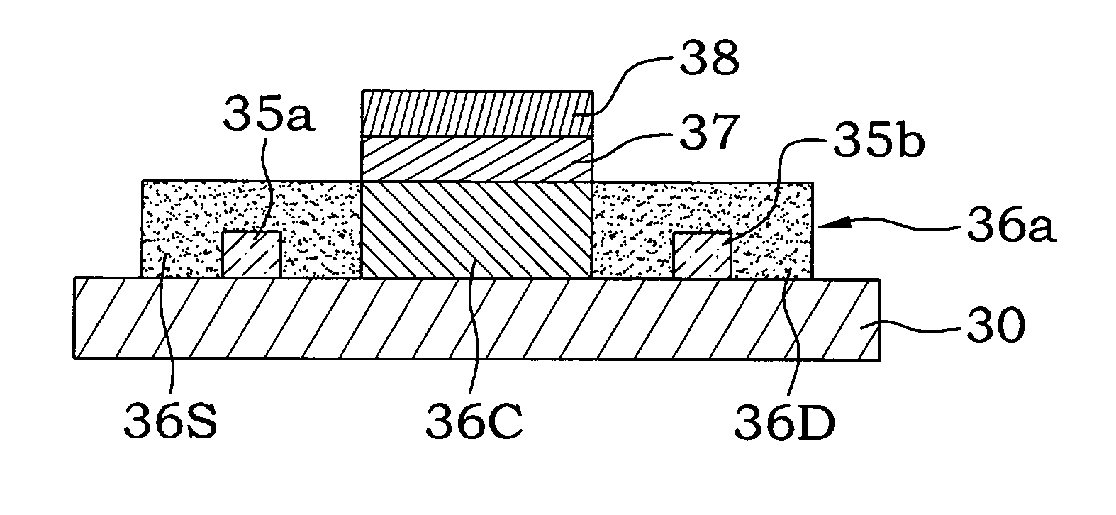
[0052]In this case, the contact mask which is essentially used for fabricating a thin film transistor (TFT) has been used in order to form the pair of island-type metal patterns 33a and 33b in the However, it is possible to form island-type metal patterns having patterns and formatting positions differing from the other embodiments in which a pair of island-type metal patterns 33a and 33b are directly deposited on an amorphous silicon thin film 31 using a separate hard mask on which holes corresponding to the pair of island-type metal patterns 33a and 33b are formed.

[0053]Also, it is also possible to form a pair of island-type metal patterns 33a and 33b in which a desired patterned photoresist pattern is formed on the crystallization induced metal film 32 according to a well-known patterning method, and the photoresist pattern is used as a mask.

[0054]Then, the amorphous silicon thin film 31 is dry-etched or wet-etched, using the island-type metal patterns 33a and 33b as an etching ...

second embodiment

[0076]FIG. 6 is a graph illustrating transfer characteristics of an N-type poly-crystalline thin film transistor fabricated by the conventional metal induced lateral crystallization (MILC) method and an N-type poly-crystalline thin film transistor fabricated by the present invention.

[0077]In the case that a drain voltage is 10V as shown in FIG. 6, an on-current is 5.2×10⁻⁵ A at a gate voltage of 20V for a thin film transistor fabricated by the conventional MILC method, and an off-current is 8.7×10⁻⁸ A at a gate voltage of −5V. Meanwhile, if a non-metal seed epitaxial growth (NSEG) method according to the second embodiment of the present invention is applied, an on-current is increased into 2.1×10⁻⁴ A and an off-current is decreased into 1.2×10⁻⁸ A. Also, in the case of the conventional MILC method, an electron mobility is eleven (11), while a thin film transistor fabricated by a NSEG method has a high electron mobility of about forty-seven (47).

[0078]This means that the N-type thin ...

third embodiment

[0084]Meanwhile, in the case of the crystallization method using the NSEG according to the present invention, it is possible to change a process so that an amorphous silicon thin film is crystallized in advance using seeds, and then all the post-processes such as formation of a gate insulation film and a gate metal film are performed. The case that an amorphous silicon film is crystallized in advance has a merit that prevents a silicon-oxide film interface characteristic from worsening due to reduction in volume of silicon at the time of crystallizing the amorphous silicon after forming the gate insulation film and the gate electrode. This will be described according to the following third embodiment of the present invention.

[0085]FIGS. 7A through 7E are cross-sectional views for explaining a method of fabricating an N-type thin film transistor according to a third preferred embodiment of the present invention.

[0086]Referring to FIG. 7A, non-metal seeds 71a and 71b are formed on a b...


PUM

PropertyMeasurementUnit
temperatureaaaaaaaaaa

Abstract

A method for crystallizing an amorphous semiconductor thin film using a non-metal seed epitaxial growth (NSEG) is provided. The method includes the steps of: forming a pair of non-metal seeds for inducing a crystallization of an amorphous semiconductor thin film at a predetermined distance on a transparent insulation substrate; depositing the amorphous semiconductor thin film on the insulation substrate; and heat-treating the insulation substrate to thereby epitaxially grow a poly-crystalline semiconductor thin film from the non-metal seeds, and to thus crystallize the amorphous semiconductor thin film. In the crystallization method, non-metal seeds are used instead of using crystallization induced metal to thereby epitaxially grow the poly-crystalline semiconductor thin film and to thus realize the amorphous semiconductor thin film without having metal pollution.

Description

BACKGROUND OF THE INVENTION[0001]1. Field of the Invention[0002]The present invention relates to a method for crystallizing an amorphous semiconductor thin film, and a method for fabricating a poly-crystalline thin film transistor using the same, and more particularly, to a method for crystallizing an amorphous semiconductor thin film, and a method for fabricating a poly-crystalline thin film transistor using the same, in which a poly-crystalline semiconductor thin film is epitaxially grown using a non-metal seed to thereby realize a crystallization of an amorphous semiconductor thin film having no metal pollution and to thus manufacture a thin film transistor having excellent characteristics.[0003]2. Description of the Related Art[0004]In general, a thin film transistor which is used in a display device such as a liquid crystal display (LCD) or an organic light emitting diode (OLED) is fabricated by processes of depositing amorphous silicon on a transparent substrate such as glass ...

Claims


Application Information

Patent Timeline
Patent Type & Authority Patents(United States)
IPC IPC(8): H01L21/00C30B29/06H01L21/20
CPCH01L21/02532H01L21/02672H01L29/66757H01L29/78675H01L27/1277
Inventor PAIK, WOON SUH
Owner PAIK WOON SUH
Why Eureka
Try Eureka