Deposition methods for barrier and tungsten materials

a technology of barrier and tungsten materials, applied in the field of semiconductor device fabrication, can solve the problems of reducing the reliability of the overall circuit, difficult to integrate cobalt silicide processes into conventional manufacturing equipment, and cobalt agglomeration

Inactive Publication Date: 2008-08-26
APPLIED MATERIALS INC
View PDF484 Cites 86 Cited by
  • Summary
  • Abstract
  • Description
  • Claims
  • Application Information

AI Technical Summary

Problems solved by technology

However, it has been difficult to integrate cobalt silicide processes into conventional manufacturing equipment.
Transfer between chambers may expose the substrate to contamination and potential oxidation of silicon or cobalt deposited on the substrate surface.
Oxide formation on the surface of the substrate can result in increasing the resistance of silicide layers as well as reducing the reliability of the overall circuit.
For example, oxidation of the deposited cobalt material may result in cobalt agglomeration and irregular growth of the cobalt silicide layer.
The agglomeration and irregular growth of the cobalt silicide layer may result in device malformation, such as source and drain electrodes having different thicknesses and surface areas.
Additionally, excess cobalt silicide growth on substrate surface may form conductive paths between devices, which may result in short circuits and device failure.
However, the addition of titanium and titanium nitride deposition and removal processes increases the number of processing steps required for silicide formation, thereby reducing process efficiency, increasing processing complexity, and reducing substrate throughput.
However, deposition of titanium over silicon surfaces presents the problem of titanium silicide formation.
Titanium silicide has been observed to agglomerate, which detrimentally affects subsequently deposited materials.
Also, titanium silicide exhibits a radical increase in sheet resistance as feature sizes decrease below 0.17 μm, which detrimentally affects the conductance of the feature being formed.
Further, titanium silicide has an insufficient thermal stability during processing of the substrate at temperatures of about 400° C. or higher, which can result in interlayer diffusion and detrimentally affect device performance.
This results in difficult integration of PVD and CVD processes in the same system.
The increase in the number of systems results in increased production costs, increased production times, and exposes the processed substrate to contamination when transferred between systems.

Method used


Image

  • Deposition methods for barrier and tungsten materials
  • Deposition methods for barrier and tungsten materials
  • Deposition methods for barrier and tungsten materials

Examples


Embodiment Construction

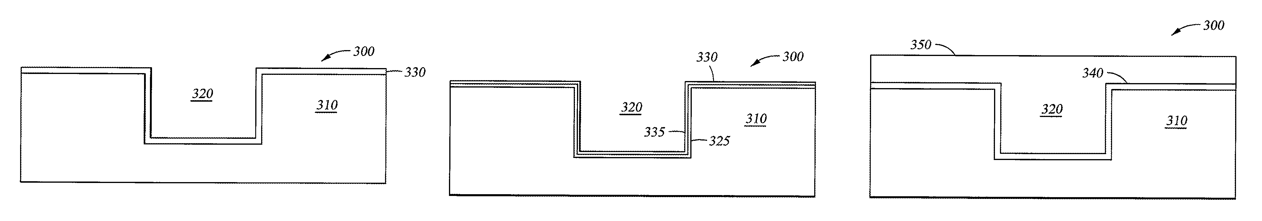
[0034]Embodiments of the invention described herein provide methods and apparatus for forming a metal silicide layer in a deposition chamber or substrate processing system. One embodiment described below in reference to a physical vapor deposition (PVD) process is provided to illustrate the invention, and should not be construed or interpreted as limiting the scope of the invention. Aspects of the invention may be used to advantage in other processes, such as chemical vapor deposition, in which an anneal is desired for forming metal silicide layers.

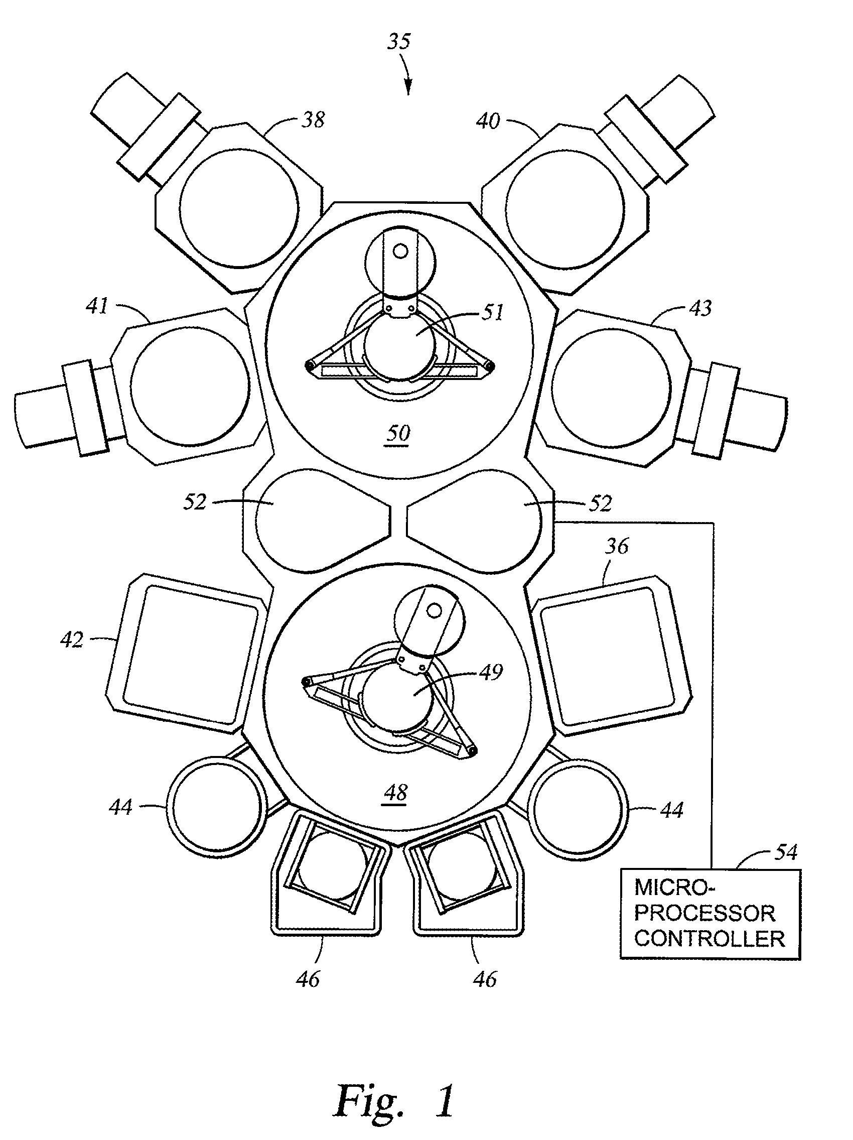
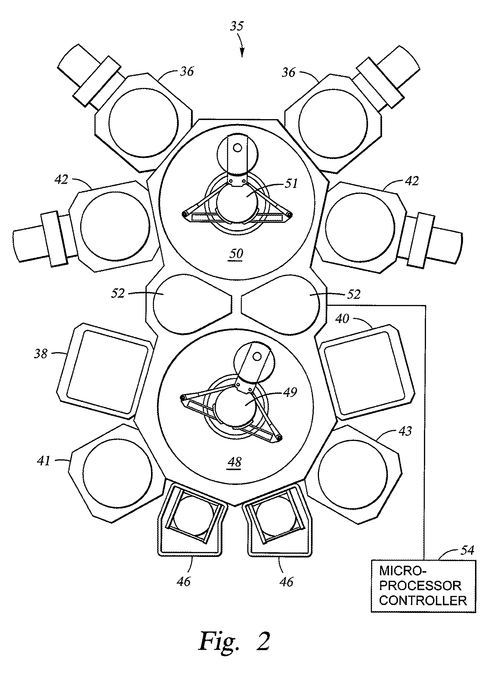
[0035]FIG. 1 shows an integrated multi-chamber substrate processing system suitable for performing at least one embodiment of the physical vapor deposition, the chemical vapor deposition, and annealing processes described herein. The deposition and annealing processes may be performed in a multi-chamber processing system or cluster tool having a PVD chamber and a CVD chamber disposed thereon. One processing platform that may be used to ad...


PUM

PropertyMeasurementUnit
sizeaaaaaaaaaa
temperaturesaaaaaaaaaa
vacuum pressureaaaaaaaaaa

Abstract

Embodiments are provided for a method to deposit barrier and tungsten materials on a substrate. In one embodiment, a method provides forming a barrier layer on a substrate and exposing the substrate to a silane gas to form a thin silicon-containing layer on the barrier layer during a soak process. The method further provides depositing a tungsten nucleation layer over the barrier layer and the thin silicon-containing layer during an atomic layer deposition process and depositing a tungsten bulk layer on the tungsten nucleation layer during a chemical vapor deposition process. In some examples, the barrier layer contains metallic cobalt and cobalt silicide, or metallic nickel and nickel silicide. In other examples, the barrier layer contains metallic titanium and titanium nitride, or metallic tantalum and tantalum nitride.

Description

CROSS-REFERENCE TO RELATED APPLICATIONS[0001]This application is a continuation of U.S. Ser. No. 10 / 845,970, filed on May 14, 2004 now abandoned, which is a continuation of U.S. Ser. No. 10 / 044,412, filed on Jan. 9, 2002, and issued as U.S. Pat. No. 6,740,585, which is a continuation-in-part of U.S. Ser. No. 09 / 916,234, which was filed on Jul. 25, 2001, now abandoned, which are all herein incorporated by reference in their entirety.BACKGROUND OF THE INVENTION[0002]1. Field of the Invention[0003]The present invention relates to the fabrication of semiconductor devices and to the apparatus and methods for deposition and annealing of materials on a semiconductor substrate.[0004]2. Description of the Related Art[0005]Recent improvements in circuitry of ultra-large scale integration (ULSI) on semiconductor substrates indicate that future generations of semiconductor devices will require sub-quarter micron multi-level metallization. The multilevel interconnects that lie at the heart of th...

Claims


Application Information

Patent Timeline
Patent Type & Authority Patents(United States)
IPC IPC(8): H01L21/00C23C14/58C23C14/06C23C16/06C23C16/24H01L21/285H01L21/768
CPCH01L21/28518H01L21/2855H01L21/28556H01L21/76864H01L21/76843H01L21/76846H01L21/76855H01L21/28562
Inventor YOON, KI HWANCHA, YONGHWA CHRISYU, SANG HOAHMAD, HAFIZ FAROOQWEE, HO SUN
Owner APPLIED MATERIALS INC
Why Eureka
Try Eureka