Semiconductor device in which zinc oxide is used as a semiconductor material and method for manufacturing the semiconductor device

a technology of semiconductor materials and semiconductor devices, which is applied in the direction of semiconductor lasers, vacuum evaporation coatings, coatings, etc., can solve the problems of unstable operation of the device, poor inability to obtain desired surface smoothness of zno thin films, etc., to achieve excellent crystallinity, excellent surface smoothness, and excellent electric characteristics

Active Publication Date: 2009-03-10
MURATA MFG CO LTD
View PDF10 Cites 3999 Cited by
  • Summary
  • Abstract
  • Description
  • Claims
  • Application Information

AI Technical Summary

Benefits of technology

[0019]To overcome the problems described above, preferred embodiments of the present invention provide a semiconductor device, which is provided with a ZnO thin film having excellent surface smoothness and which has excellent crystallinity and excellent electric characteristics, and a method for manufacturing the semiconductor device.
[0020]The inventors of the present invention conducted intensive research in order to obtain a ZnO thin film having excellent surface smoothness. As a result, it was discovered that a semiconductor device having excellent surface smoothness and crystallinity and excellent electric characteristics could be obtained by forming a ZnO thin film on a zinc-polar surface of a single crystal substrate, primarily including zinc oxide.
[0021]A semiconductor device according to a preferred embodiment of the present invention includes a single crystal substrate primarily including zinc oxide which has a zinc-polar surface and an oxygen-polar surface and at least one layer of thin film primarily including zinc oxide is disposed on the above-described zinc polar surface. In this manner, a thin film having excellent surface smoothness and crystallinity is produced.

Problems solved by technology

However, substantially hexagonal crystal grains remain in such a ZnO film, the surface shape becomes uneven and, thereby, the desired surface smoothness of the ZnO thin film cannot be obtained.
That is, since the ZnO thin film formed by the first known technology has poor surface smoothness, where a semiconductor device is formed using the ZnO thin film, a current passes through grain boundaries, and a concentration of electric field occurs on convex portions of crystal grains.
Consequently, the operation of the device may become unstable, or the device may be destroyed.
Furthermore, it is difficult to control the above-described diffusion and, therefore, variations may occur in the device characteristics of the semiconductor device.
As a result, the crystallinity of the ZnO thin film is deteriorated and, thereby, deterioration of the electric characteristics occurs.
However, there is no disclosure with respect to the influence exerted by the polarity on the surface shape and the electric characteristics of the thin film.
Furthermore, since the material for the substrate is different from the material for the piezoelectric film, deterioration of the crystallinity may occur due to the lattice mismatch as in the second known technology, and there is a problem in that highly reliable, desirable, and excellent electric characteristics cannot be obtained.

Method used


Image

  • Semiconductor device in which zinc oxide is used as a semiconductor material and method for manufacturing the semiconductor device
  • Semiconductor device in which zinc oxide is used as a semiconductor material and method for manufacturing the semiconductor device
  • Semiconductor device in which zinc oxide is used as a semiconductor material and method for manufacturing the semiconductor device

Examples


Embodiment Construction

[0044]Preferred embodiments of the present invention will be described below in detail with reference to the drawings.

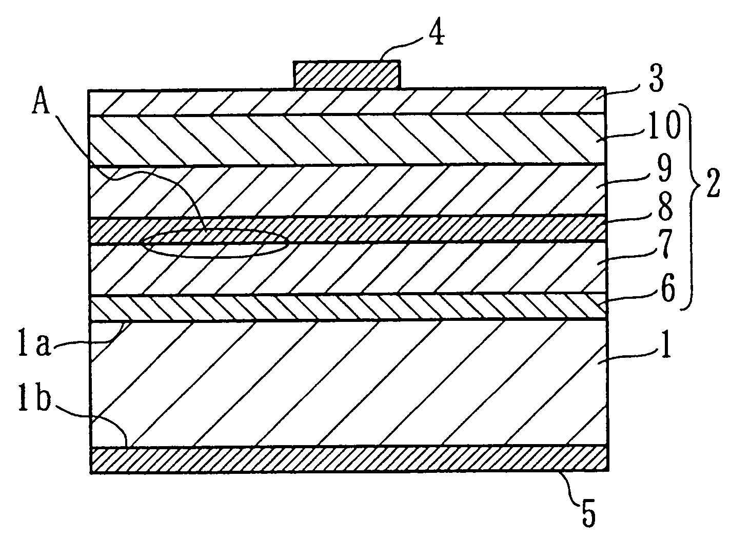
[0045]FIG. 1 is a schematic sectional view of a Light Emitting Diode (hereafter referred to as “LED”) as a first preferred embodiment of a semiconductor device according to the present invention.

[0046]In FIG. 1, reference numeral 1 denotes a single crystal substrate primarily including electrically conductive ZnO having an n-type conduction form (hereafter referred to as “ZnO substrate”), and the ZnO substrate 1 has a zinc-polar surface 1a and an oxygen-polar surface 1b.

[0047]In the LED, a light-emitting layer 2 is disposed on the zinc-polar surface 1a of the ZnO substrate 1, and a transparent electrode 3 made of Indium Tin Oxide (hereafter referred to as “ITO”) and having a film thickness of about 150 nm is disposed on the surface of the light-emitting layer 2. Furthermore, a p-side electrode 4 having a total film thickness of about 300 nm is disposed on a substant...


PUM

PropertyMeasurementUnit
thicknessaaaaaaaaaa
thicknessaaaaaaaaaa
thicknessaaaaaaaaaa

Abstract

A semiconductor device having excellent crystallinity and excellent electric characteristics includes a ZnO thin film having excellent surface smoothness. ZnO-based thin films (an n-type contact layer, an n-type clad layer, an active layer, a p-type clad layer, and a p-type contact layer) primarily including ZnO are formed sequentially by an ECR sputtering method or other suitable method on a zinc-polar surface of a ZnO substrate. A transparent electrode and a p-side electrode are formed by an evaporation method or other suitable method on a surface of the p-type contact layer, and an n-side electrode is formed on an oxygen-polar surface of the ZnO substrate.

Description

BACKGROUND OF THE INVENTION[0001]1. Field of the Invention[0002]The present invention relates to a semiconductor device and a method for manufacturing the semiconductor device. In particular, the present invention relates to a semiconductor device in which zinc oxide is used as a semiconductor material and to a method for manufacturing the semiconductor device.[0003]2. Description of the Related Art[0004]Zinc oxide (ZnO) is one type of II-VI compound semiconductor. The band gap energy of ZnO can be changed by making ZnO into a mixed crystal with MgO, CdO, or other suitable materials, and ZnO can have a multilayer structure of quantum well and other suitable structures. Furthermore, since the bond energy of an exciton is very large, ZnO is suitable for use in light-emitting devices. Since ZnO is transparent in the visible range, ZnO is also suitable for use in transparent thin film transistors for driving liquid crystal displays.[0005]Meanwhile, ZnO has a wurtzite structure (hexagona...

Claims


Application Information

Patent Timeline
Patent Type & Authority Patents(United States)
IPC IPC(8): H01L29/24H01L21/00C23C14/08C23C16/40H01L21/36H01L21/363H01L29/786H01L33/18H01L33/28H01L33/42H01S5/327H01S5/347
CPCH01L29/7869H01L33/28H01S5/327H01L21/02403H01L21/02472H01L21/02483H01L21/02507H01L21/02554H01L21/02565H01L21/02581H01L21/02631
Inventor ITO, YOSHIHIROKADOTA, MICHIO
Owner MURATA MFG CO LTD
Why Eureka
Try Eureka