Method of changing an energy attenuation factor of a linear light in order to crystallize a semiconductor film

a technology of energy attenuation factor and linear light, which is applied in the direction of laser beam welding apparatus, welding apparatus, manufacturing tools, etc., can solve the problems of not being able to hold such information, unable to achieve improvement at a temperature lower, and using a cw laser, etc., to achieve small off-current, large mobility, and small size

Inactive Publication Date: 2009-05-05
SEMICON ENERGY LAB CO LTD
View PDF50 Cites 4 Cited by
  • Summary
  • Abstract
  • Description
  • Claims
  • Application Information

AI Technical Summary

Benefits of technology

[0032]An object of the present invention is to provide, by solving the above problems, a laser illumination system which can perform illumination at constant laser energy even using a pulsed oscillation laser.
[0033]Another object of the invention is to provide an apparatus which allows the above-described laser light illumination method to be performed in short time in a simple way.
[0039]The laser illumination system having the above configuration enables formation of a silicon film having regions of different electrical characteristics on the same substrate by changing the laser light illumination energy. Further, by using the above-described energy attenuating device, it becomes possible to perform laser processing with throughput equivalent to that as would be obtained when laser illumination is conducted without changing the laser light illumination energy. By forming a number of TFTs on the thus-produced silicon film, TFTs having a large mobility and TFTs having a small off-current can be formed on the same substrate. By using this technique, an active matrix liquid crystal display device can be constructed in which the peripheral circuit area is constituted of TFTs having a large mobility and the pixel area is constituted of TFTs having a small off-current.

Problems solved by technology

If semiconductor devices in the pixel area do not have a sufficiently small off-current, they cannot hold such information.
On the other hand, almost no improvement is obtained at a temperature lower than 500° C. Therefore, to decrease the process temperature, it is necessary to replace a conventional thermal annealing step with some other proper step.
The first method of using a CW laser has a problem of long processing time, because the maximum energy of the CW laser is insufficient and therefore the beam spot size is at most several millimeters.
The remaining problem is insufficient uniformity of laser light illumination effects.
In particular, when illumination is performed in an energy range where stable laser oscillation cannot be obtained easily, it is difficult to perform laser processing with uniform energy over the entire substrate surface.
Another problem associated with the use of a pulsed oscillation laser is that the laser light energy decreases as the laser is used over a long time, which attributes to degradation of a gas necessary for laser oscillation.
However, in practice, raising the operation level is not preferable because once the operation level is changed, it takes some time for the laser light energy to be stabilized.
By the way, it is conventionally very difficult to produce, only with laser light illumination, a crystalline silicon film having such a large mobility as enables fast operation of a liquid crystal display.
The variation of off-current values adversely affect the pixels, and causes point defects and line defects in a completed liquid crystal display.
As described above, a pixel-to-pixel variation of the off-current in the pixel area causes fatal defects for the operation of a liquid crystal display.
However, it has been proved that a variation of off-current values of thin-film transistors disposed in the peripheral circuit area does not have large influences on the operation of a liquid crystal display.
However, the scheme of individually applying laser beams of different energies to the peripheral circuit area and the pixel area makes the laser light illumination step complex and time-consuming.
For example, if the peripheral circuit area is illuminated while the pixel area is masked, and vice versa, this process takes long time and becomes complex because of two times of illumination.

Method used


Image

  • Method of changing an energy attenuation factor of a linear light in order to crystallize a semiconductor film
  • Method of changing an energy attenuation factor of a linear light in order to crystallize a semiconductor film
  • Method of changing an energy attenuation factor of a linear light in order to crystallize a semiconductor film

Examples


embodiment 1

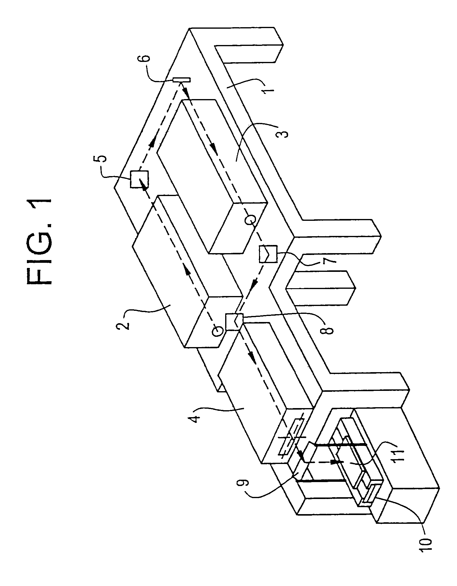
[0048]First of all, a description will be made of an apparatus. FIG. 1 shows the concept of a laser annealing apparatus used in this embodiment. Reference numeral 1 denotes a main body of the laser annealing apparatus. An oscillator 2 emits KrF excimer laser light (wavelength: 248 nm; pulse width: 25 ns). Apparently other excimer lasers and other types of laser may also be used.

[0049]Laser light emitted from the oscillator 2 is reflected by full-reflection mirrors 5 and 6, amplified by an amplifier 3, reflected by full-reflection mirrors 7 and 8, and introduced into an optics 4. Although not shown in FIG. 4, an energy attenuating device is inserted between the mirror 8 and the optics 4. FIG. 3 shows the configuration of the energy attenuating device.

[0050]As shown in FIG. 3, the energy attenuating device is of a type in which a single plate of filter faces a traveling laser beam and the energy transmission factor is changed by changing the angle formed by the beam and the filter.

[00...

embodiment 2

[0057]Although the mirror G being partially transmissive. provides the advantage of real-time measurement of the laser light illumination energy (first embodiment; FIG. 1), it has a disadvantage that part of the laser energy is lost. This embodiment is directed to an apparatus for solving that problem. However, the apparatus of this embodiment cannot measure the energy of the linear laser beam on a real-time basis.

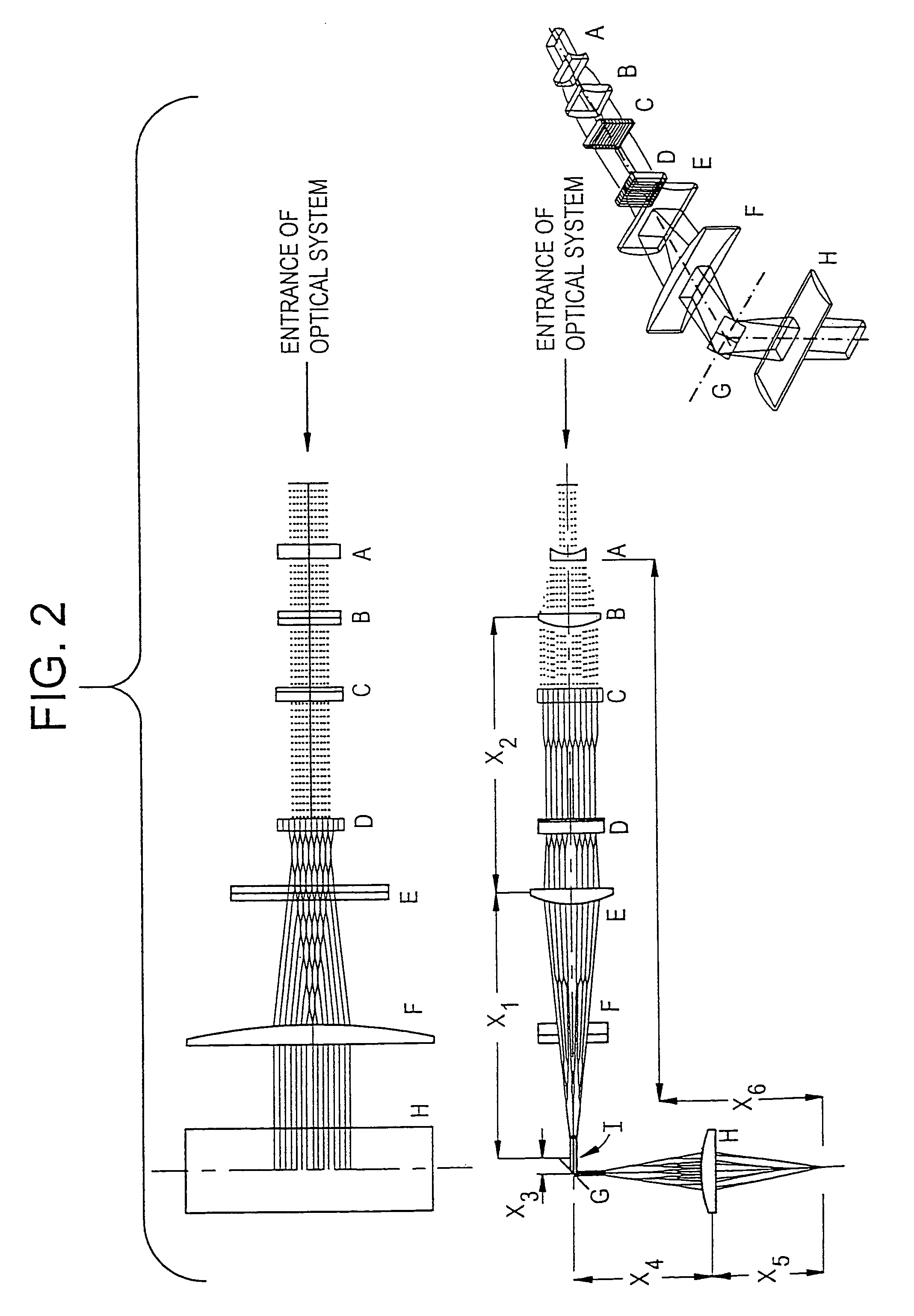
[0058]FIG. 5 shows a laser light illuminating portion of the apparatus of this embodiment. A mirror P in FIG. 5 corresponds to the mirror G in FIG. 1. The mirror P is a full-reflection mirror, and a 4%-reflection mirror Q is disposed under the mirror P. An energy component reflected by the mirror Q enters a beam profiler R. The mirror Q is smaller than the mirror P, because the beam profiler measures a small area each time. The mirror Q moves in link with the beam profiler R, and is adapted to slide over a range longer than the linear laser beam. During laser light illumin...

embodiment 3

[0059]We have studied the method for improving the crystallinity of an amorphous or crystalline silicon or silicon compound film by illuminating it with laser light and, in particular, the manufacturing method of a film suitable as a material for a liquid crystal display device, and propose the following apparatus that facilitates manufacture of such a film.

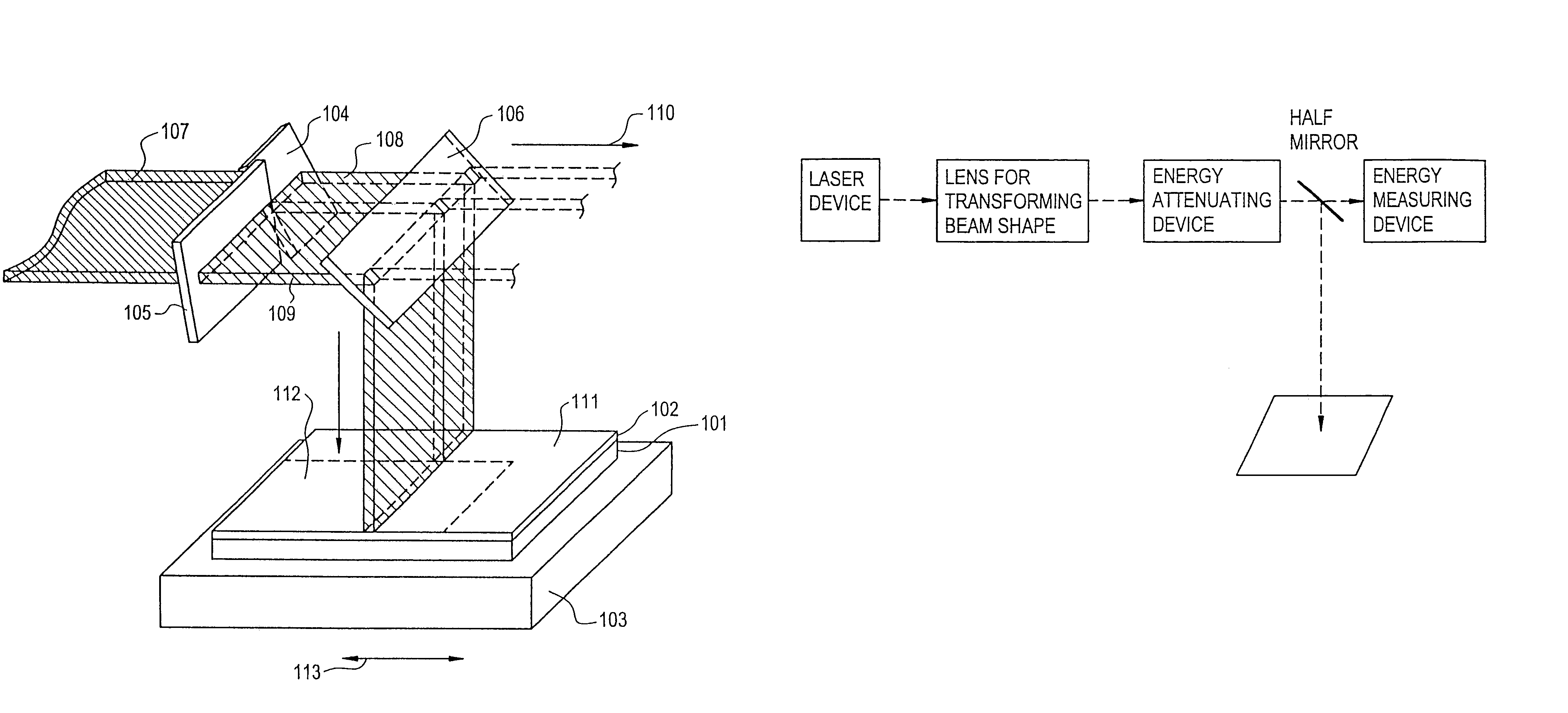
[0060]As in the first embodiment, this embodiment uses the laser annealing apparatus shown in FIG. 1. An energy attenuating device is inserted into the output-side optical path of the optics 4 of FIG. 1. FIG. 6 shows the configuration of the energy attenuating device. A brief description will be made of the mechanism of this device. Referring to FIG. 6, the light attenuation factor of each of special light attenuation filters 104 and 105 is changed by changing the angle formed by the laser beam and the filter. The transmission factor of each of the light attenuation filters 104 and 105 is maximum when the filter is perpendicular ...


PUM

PropertyMeasurementUnit
temperatureaaaaaaaaaa
wavelengthaaaaaaaaaa

Abstract

The illumination energy of an excimer laser is measured and adjusted to always effect illumination at constant energy. A laser beam output from an optics is reflected by a mirror, and applied to a sample. A beam profiler is disposed behind the mirror to measure the energy of an illumination laser beam. An energy attenuating device disposed between another mirror and the optics is operated based on the measurement value so that the energy of the laser beam applied to the sample is kept constant.

Description

BACKGROUND OF THE INVENTION[0001]1. Field of the Invention[0002]The present invention relates to the configuration of a laser apparatus used for a semiconductor device manufacturing process and other purposes. In particular, the invention relates to a laser apparatus used to improve or restore, by application of laser light, the crystallinity of a semiconductor material partially or fully made of an amorphous component, a substantially intrinsic, polycrystalline semiconductor material, or a semiconductor material whose crystallinity has been lowered being damaged by ion application, ion implantation, ion doping, or the like.[0003]The invention also relates to a laser illumination system used for a low-temperature process for producing TFTs that are used in a liquid crystal display device and, more specifically, to a technique for forming, on the same substrate, thin-film transistors having a large mobility disposed in a peripheral circuit area and a number of thin-film transistors h...

Claims


Application Information

Patent Timeline
Patent Type & Authority Patents(United States)
IPC IPC(8): H01L21/00B23K26/073B23K26/42
CPCB23K26/0732B23K26/422B23K26/702
Inventor YAMAZAKI, SHUNPEITANAKA, KOICHIRO
Owner SEMICON ENERGY LAB CO LTD
Why Eureka
Try Eureka