Electronic device with dopant diffusion barrier and tunable work function and methods of making same

a technology of electronic devices and diffusion barriers, applied in the direction of basic electric elements, semiconductor devices, electrical equipment, etc., can solve the problems of device performance, limiting effects, and significant engineering challenges involving dopant diffusion, and achieve the effect of preventing depletion effects

Active Publication Date: 2009-11-03
ATMEL CORP
View PDF13 Cites 4 Cited by
  • Summary
  • Abstract
  • Description
  • Claims
  • Application Information

AI Technical Summary

Benefits of technology

[0013]An embodiment of the present invention is therefore a method of forming an MOS gate electrode comprising a diffusion-blocking layer made substantially of silicon, germanium, and carbon. The diffusion-blocking layer prevents dopant penetration into or across the gate dielectric and allows in-situ doping of the gate to further prevent depletion effects. The method includes in-situ doping of select portions of the gate stack with various n-type and p-type impurities. The method also includes germanium profile tailoring thus allowing engineering of the work function and the dopant diffusion. A specific exemplary method includes forming a silicon seed layer over a gate dielectric, depositing an in-situ doped polysilicon germanium diffusion-blocking layer containing carbon, followed by deposition and in-situ doping of the main gate layer, and finally depositing a silicon contact layer. The diffusion-blocking layer contains a higher level of germanium than the main layer and the Ge profile in the diffusion-blocking layer is generally that of a trapezoid.

Problems solved by technology

As device geometries continue to scale downward, issues involving dopant diffusion have become a significant engineering challenge.
Among these challenges is limiting effects related to gate depletion and dopant penetration of a thin gate dielectric.
Gate depletion and dopant penetration lead to device performance issues related to changes in threshold voltage or turn-on voltage of a transistor and also relate to sub-threshold leakage current or inability to completely turn the transistor off.
In PMOSFETs, the dopant penetration will shift the threshold voltage from negative to positive, making it difficult or impossible to turn the transistor off.
Another cause of the depletion region is an inability of ion implantation and subsequent thermal anneal process steps to result in a homogeneously doped layer from top to bottom.
Unfortunately, any occurrence of a depletion region in the gate electrode tends to degrade transistor performance.
The dopant penetration also causes device performance degradation related to changes in both threshold voltage and sub-threshold leakage.
Additionally, the dopant should not be allowed to penetrate into the gate dielectric layer.
However, problems of gate depletion and gate penetration are still not completely resolved by the addition of Ge to the polysilicon layer.
The gate depletion problem still exists due to inhomogeneous doping throughout the poly layers as a result of an ion implantation profile, as well as the gate penetration problem associated with ion implantation straggle.

Method used


Image

  • Electronic device with dopant diffusion barrier and tunable work function and methods of making same
  • Electronic device with dopant diffusion barrier and tunable work function and methods of making same
  • Electronic device with dopant diffusion barrier and tunable work function and methods of making same

Examples


Embodiment Construction

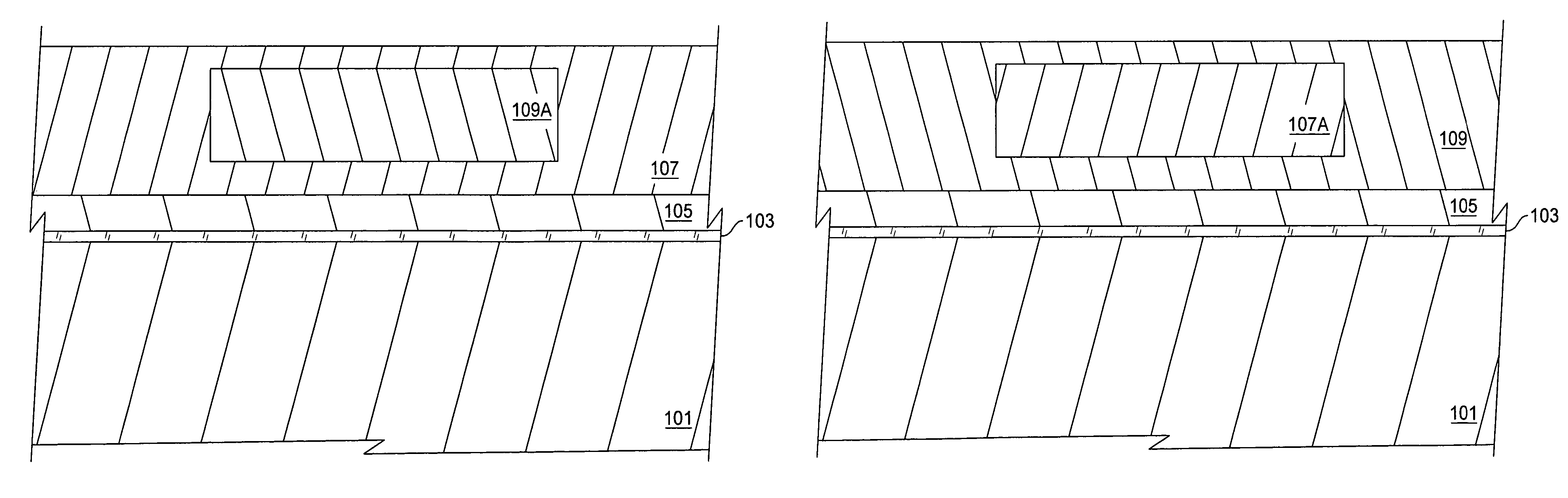
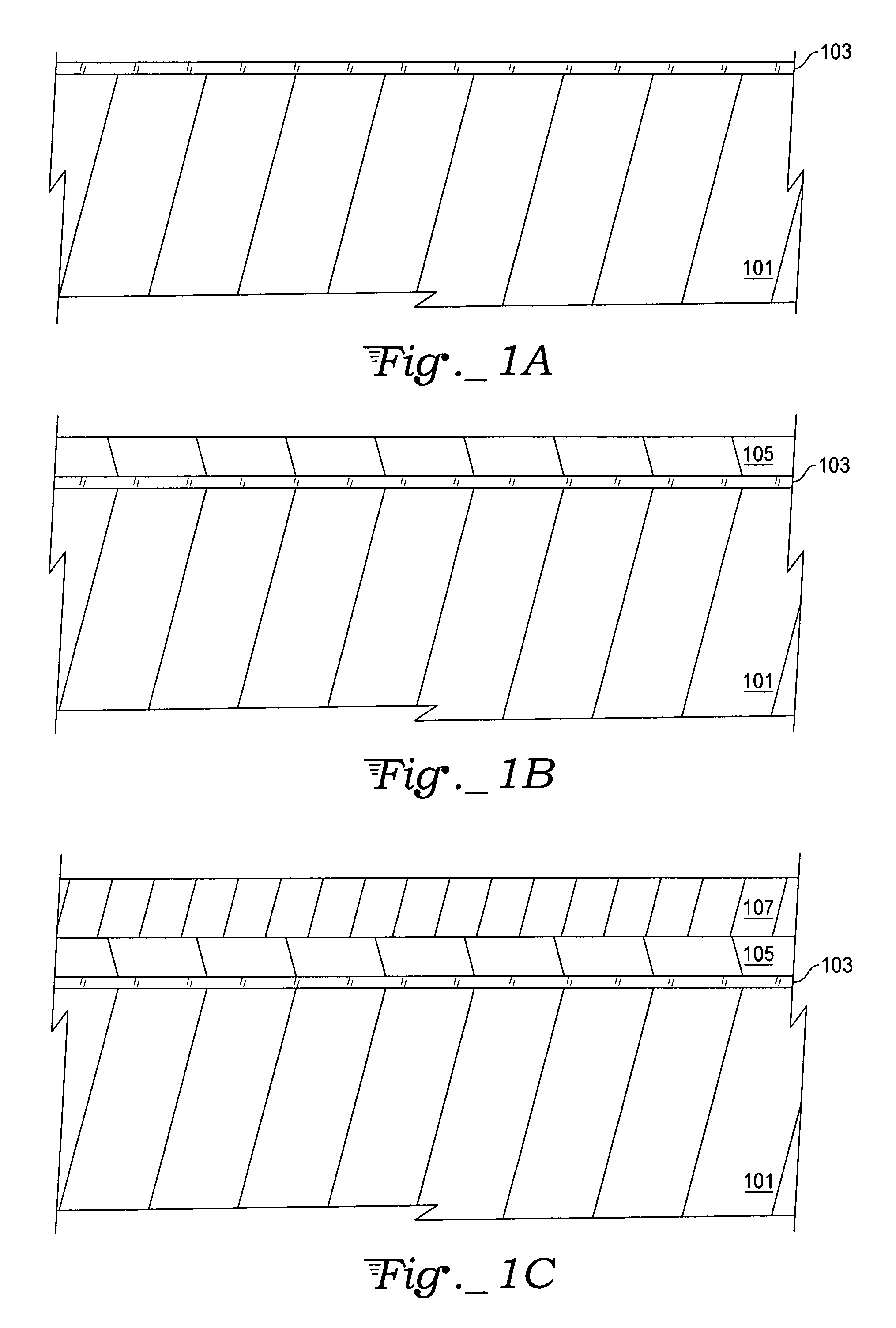
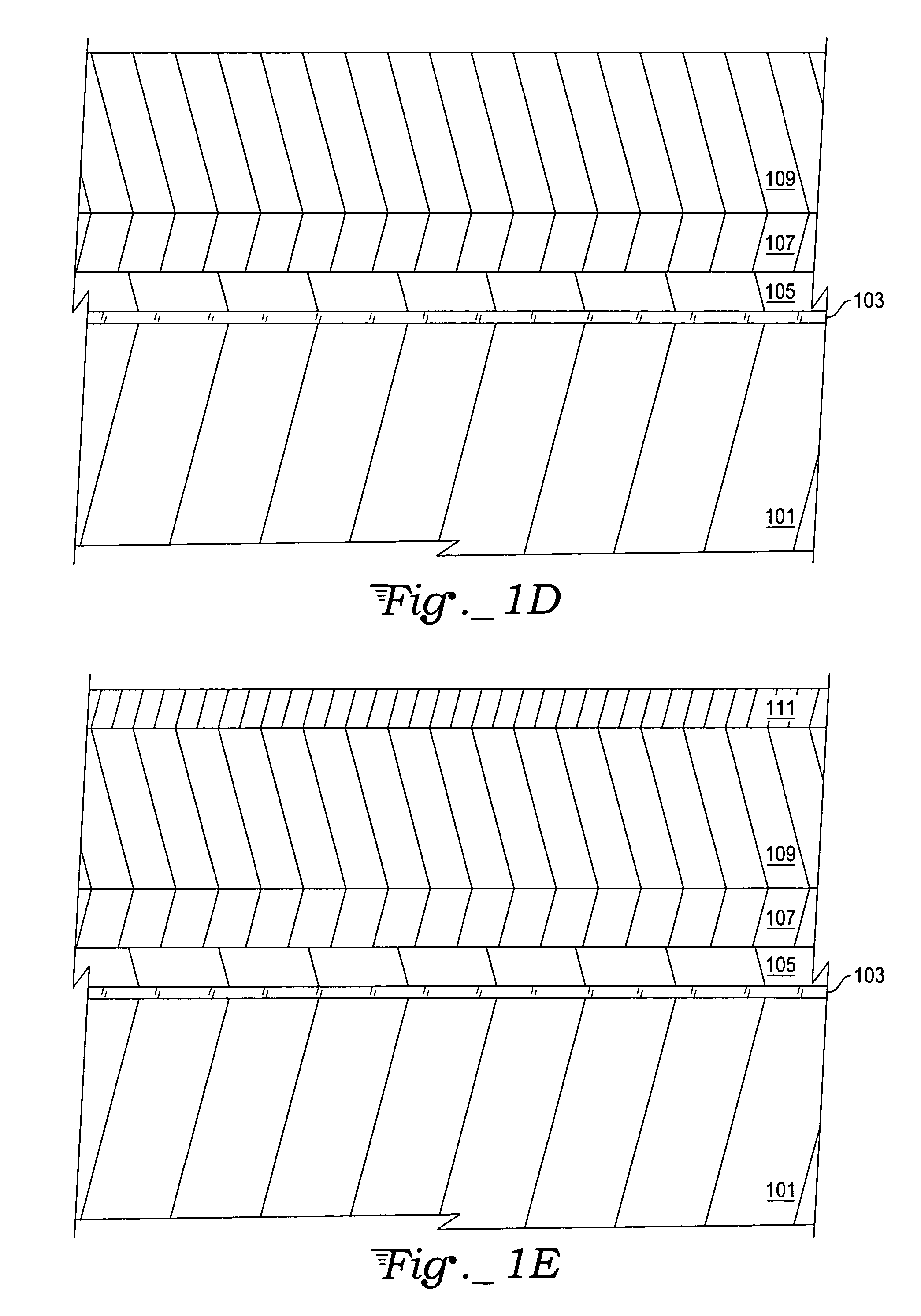
[0022]With reference to FIGS. 1A-1E, overall exemplary process steps of a polysilicon germanium gate electrode illustrate diffusion-blocking techniques of the present invention. For simplicity, a single MOS transistor is illustrated with source and drain regions truncated. Formation of the gate electrode will take place upon a gate dielectric film. The gate dielectric film is deposited or otherwise formed upon a substrate. The MOS transistor may be of either a p-type or an n-type conductivity. Further, one skilled in the art will recognize that the exemplary process steps described herein are readily amenable to other processes and types of electronic devices.

[0023]FIG. 1A is a cross-section of a MOS capacitor constructed up to the gate dielectric and includes a substrate 101 and a gate dielectric 103. In a specific exemplary embodiment, the substrate 101 is a p-type silicon wafer and the gate dielectric 102 is comprised of silicon dioxide. Alternatively, the substrate 101 could als...


PUM

PropertyMeasurementUnit
dielectric thicknessaaaaaaaaaa
thicknessaaaaaaaaaa
thicknessaaaaaaaaaa

Abstract

A method of fabricating a semiconductive film stack for use as a polysilicon germanium gate electrode to address problems associated with implant and diffusion of dopants. Achieving a sufficiently high active dopant concentration at a gate-dielectric interface while avoiding gate penetration of dopants such as boron is problematic. A higher gate implant dosage or annealing temperature is needed, and boron penetration through the thin gate oxide is inevitably enhanced. Both problems are exacerbated as the gate dielectric becomes thinner. In order to achieve a high level of active dopant concentration next to the gate dielectric without experiencing problems associated with gate depletion and penetration, a method and procedures of applying a diffusion-blocking layer is described with respect to an exemplary MOSFET application. However, a diffusion-blocking concept is also presented, which is readily amenable to a variety of semiconductor related technologies.

Description

TECHNICAL FIELD[0001]The invention generally relates to methods of fabrication of integrated circuits (ICs). More specifically, the invention is a method of fabricating a metal-oxide-silicon (MOS) gate electrode containing a diffusion-blocking layer made substantially of silicon and germanium.BACKGROUND ART[0002]Polysilicon germanium (poly-SiGe) is advantageous over polysilicon as a gate electrode material due to its reduced dopant diffusion properties and work function engineering capability. Consequently, poly-SiGe films have gained much attention for design and manufacturing of MOS devices.[0003]Advances in semiconductor manufacturing technology have allowed integration of hundreds of millions of circuit elements, such as transistors, on a single integrated circuit (IC). In order to achieve such increases in density, interconnect line widths become smaller and overall dimensions of metal-oxide-semiconductor field effect transistors (MOSFETs) have decreased. These transistor devic...

Claims


Application Information

Patent Timeline
Patent Type & Authority Patents(United States)
IPC IPC(8): H01L29/43
CPCH01L21/2807
Inventor ENICKS, DARWIN G.
Owner ATMEL CORP
Why Eureka
Try Eureka