Method of introducing ion and method of manufacturing semiconductor device

a technology of semiconductor devices and ionization, which is applied in the direction of semiconductor devices, basic electric elements, electrical appliances, etc., can solve the problems of difficult to completely remove resists, uneven quantity of ion to be introduced in semiconductor devices, and deterioration of semiconductor properties, so as to reduce or prevent the introduction of components, reduce the weight of the target, and improve the effect of durability

Inactive Publication Date: 2009-11-10
SEMICON ENERGY LAB CO LTD
View PDF23 Cites 0 Cited by
  • Summary
  • Abstract
  • Description
  • Claims
  • Application Information

AI Technical Summary

Benefits of technology

[0026]In the above-described method, it is desirable that a silicon film is used as the semiconductor. Further, compound semiconductor films each having an amorphous structure such as an amorphous silicon film, as well as an amorphous silicon germanium film may be applied. Further, as substrates for forming the semiconductor, for example, a glass substrate, a quartz substrate, a silicon substrate, a plastic substrate, a metal substrate, a stainless-steel substrate, and a flexible substrate can be used. Examples of the glass substrates include substrates made of glasses such as a barium borosilicate glass and an alumino-borosilicate glass. Further, examples of the flexible substrates include substrates each in a film state made of PET, PES, PEN, and an acrylic resin. When the semiconductor device is manufactured by using the flexible substrate, manufacturing of the device having a lighter weight can be aimed. It is desirable that, when a barrier layer such as an aluminum film (such as AlON, AlN, or AlO), an carbon film (such as DLC (diamond-like carbon)) or SiN is formed on a front surface, or a front surface and a rear surface of the flexible substrate in a single layer or multi-layer manner, durability is enhanced.
[0027]As described above, according to the invention, by performing the introduction of the ion by dividing the introduction processing itself into a plurality of times, it becomes possible to decrease or prevent the introduction of a component of the dissociated gas into the semiconductor. Further, the introduction of the ion into the semiconductor can be performed without departing from the set conditions and in a uniform manner. Still further, since baking processing is not performed on the resist before the ion is introduced, a number of processing steps is not increased and, also, it becomes possible to easily perform a removal of the resist which is to be conducted after the ion is introduced. These features are highly effective factors in a recent trend in which the size of the substrate is being enlarged.
[0028]By applying the method according to the invention, in a semiconductor device, which is represented by an active matrix-type liquid crystal display device, enhancements of operational characteristics and reliability of the semiconductor device can be achieved. Still further, lowering a production cost of the semiconductor device can be achieved.

Problems solved by technology

Further, since the resist is partially formed on the semiconductor, the dissociated gas is locally generated to cause a quantity of ion to be introduced in the semiconductor to be unevenly distributed.
Furthermore, since pressure inside a treatment chamber in which the introduction of the ion is performed varies due to the generation of the dissociated gas, arcing may sometimes appear, or an ion density or an acceleration voltage is adversely affected to allow the ion introduction conditions to depart from the set ion introduction conditions.
This is a serious problem in a recent trend in which a size of a substrate is being enlarged and also becomes a major factor of deteriorating semiconductor properties.
However, it is sometimes difficult to completely remove the resist which has been cured by the baking processing or the UV irradiation even with ashing, peeling, or other appropriate processing.
Since the resist is ordinarily an organic film, when the resist remains on the semiconductor as a residue, an apparatus to be used in a subsequent step in the introduction of the ion is contaminated whereupon such contamination will cause deterioration of not only properties of the semiconductor of interest but also properties of other semiconductors and will, then, give a detrimental effect on operating characteristics of the semiconductor device.
Further, such contamination will deteriorate a coating property of a film to be formed after the ion is introduced whereupon such deterioration may cause a malfunction such as wire breakage.
Furthermore, performing the baking processing or the UV irradiation increases a number of processing steps to thereby cause an increase of an overall processing time or cost.

Method used


Image

  • Method of introducing ion and method of manufacturing semiconductor device
  • Method of introducing ion and method of manufacturing semiconductor device
  • Method of introducing ion and method of manufacturing semiconductor device

Examples


example 1

[0044]Embodiments according to the present invention are described in detail with reference to FIGS. 1A to 1C.

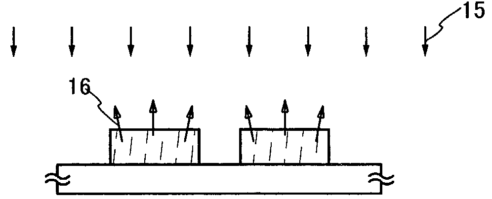
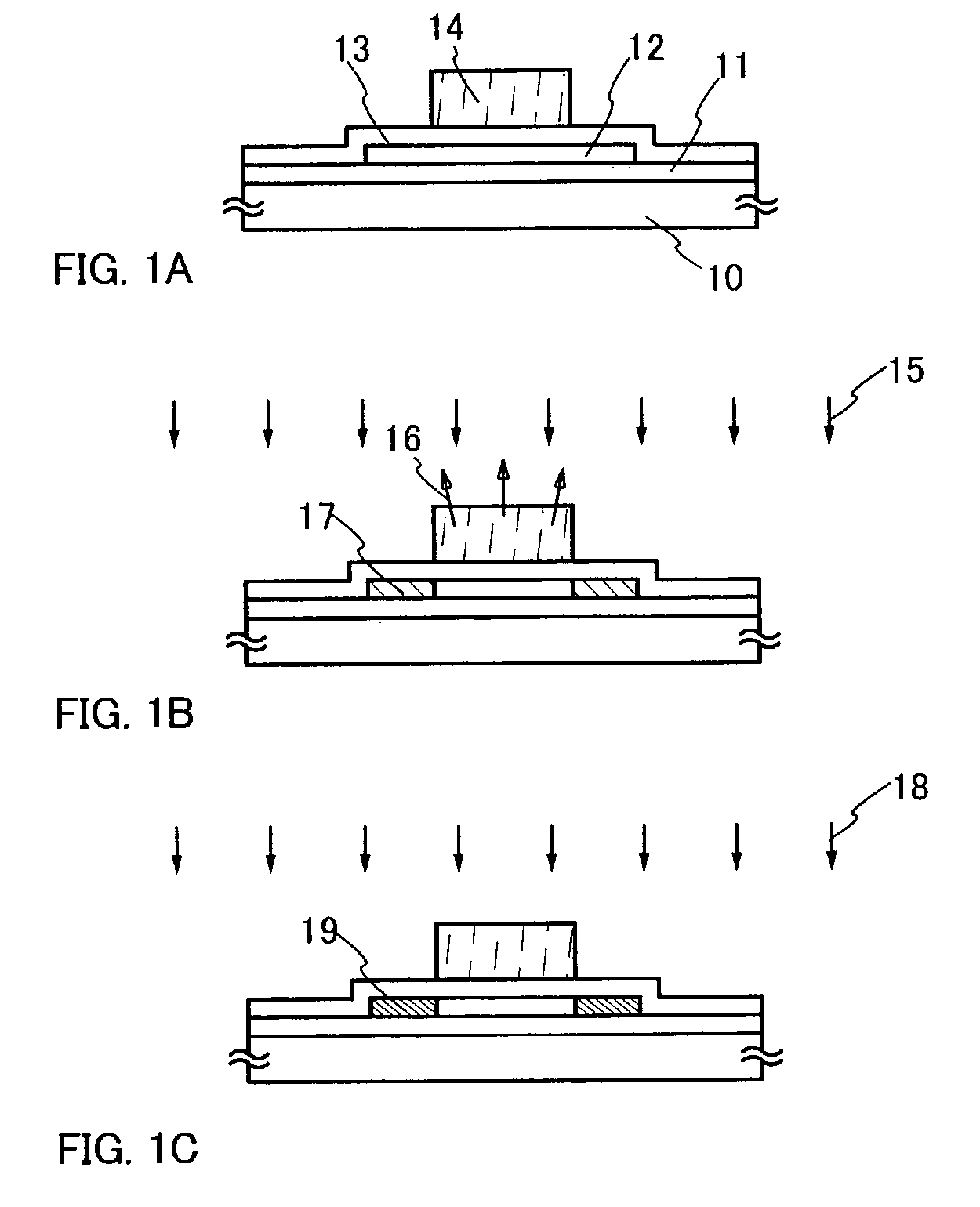
[0045]FIG. 1A shows an example of a semiconductor on which a resist is partially formed. An underlying insulating film 11 is formed on a substrate 10 and, then, a semiconductor film 12 is formed on the thus-formed underlying insulating film 11 and, thereafter, a resist 14 is formed on the thus-formed semiconductor film 12 via an insulating film 13. It goes without saying that the resist 14 may be formed on the semiconductor film 12 without forming the insulating film 13 therebetween.

[0046]A first introduction of a first ion 15 into the semiconductor on which the resist 14 is thus formed is performed by a first acceleration voltage. In such first introduction processing, an apparatus such as an ion-doping apparatus or an ion implantation apparatus may be used and, also, a known material gas (for example, PH3, B2H6) may be used as a material gas. Further, an inert gas which wi...

example 2

[0053]In the present Example, described is a result obtained by observing changes of pressure inside a treatment chamber when a resist was formed on a substrate and, then, a first introduction of an ion and a second introduction of an ion were performed. Further, in the Example, an experiment was conducted while a condition of a first acceleration voltage was fluctuated at the time of the first introduction.

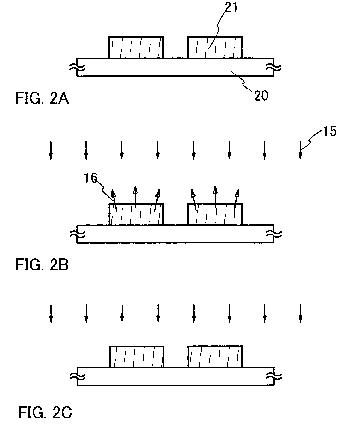
[0054]FIGS. 2A to 2C show an example in which a resist 21 is partially formed on a substrate 20. In this example, a glass substrate was used as the substrate 20 and a novolac resin was used as the resist 21.

[0055]A first introduction of the ion was performed into the substrate on which the resist 21 was thus formed. Such introduction processing was performed for 6 minutes by using an ion doping apparatus and B2H6 as a material gas. Further, 3 types of acceleration voltages, that is, 10 kV, 40 kV, and 90 kV, were adopted. Changes of the pressure inside the treatment chamber under ...

example 3

[0061]In the present Example, described is a result obtained by observing changes of pressure inside a treatment chamber when a resist was formed on a substrate and, then, a first introduction of an ion and a second introduction of an ion were performed. Further, in the Example, a condition of a second acceleration voltage was fluctuated at the time of the second introduction.

[0062]FIGS. 2A to 2C show an example in which a resist 21 is partially formed on a substrate 20. In this example, a glass substrate was used as the substrate 20 and a novolac resin was used as the resist 21.

[0063]A first introduction of the ion was performed into the substrate on which the resist 21 was thus formed. Such introduction processing was performed for 6 minutes by using an ion doping apparatus and B2H6 as a material gas. Further, a radio frequency supply of 5 W and an acceleration voltage of 90 kV were adopted. Changes of the pressure inside the treatment chamber under the above-described conditions ...


PUM


Abstract

When an ion is introduced into a semiconductor on which a resist is formed, the ion and the resist react with each other to generate a gas (dissociated gas) and a component of the thus-generated dissociated gas is introduced into the semiconductor, which becomes a factor to deteriorate properties of the semiconductor. According to the invention, the dissociated gas to be generated from an organic film is treated. Particularly, the dissociated gas is treated before an ion introduction is performed. As a method of performing such a treatment, the ion introduction is performed by dividing ion introduction processing itself into a plurality of times. The dissociated gas is generated in a maximum quantity just after the ion introduction is started. For this reason, it is possible to decrease an introduction of a component of the dissociated gas into the semiconductor or prevent the component of the dissociated gas from being introduced into the semiconductor, when ion introduction processing is divided into a plurality of times and, in each of the thus-divided ion introduction processing after a second time thereof, the ion is introduced while removing the dissociated gas from a treatment chamber by performing evacuation.

Description

BACKGROUND OF THE INVENTION[0001]1. Field of the Invention[0002]The present invention relates to a method of introducing an ion. Further, the present invention also relates to a method of manufacturing a semiconductor device which is manufactured by a step comprising introducing an ion. As used herein, the term “semiconductor device” is intended to include all devices which can exert functions thereof by making use of semiconductor characteristics. It is construed that the term “semiconductor device” is further intended to include in the category thereof other devices, such as a liquid crystal display device in which a thin film transistor and liquid crystal are combined with each other, and a light emitting device in which a thin film transistor and a light emitting element are combined with each other.[0003]2. Description of the Related Art[0004]A technique for manufacturing a circuit having a predetermined function by first forming an element such as a thin film transistor on a s...

Claims


Application Information

Patent Timeline
Patent Type & Authority Patents(United States)
IPC IPC(8): H01L21/08H01L21/336H01L21/77H01L21/84H01L27/12
CPCH01L29/66757H01L27/1214H01L27/127H01L27/1255
Inventor HAYAKAWA, SHIGENORI
Owner SEMICON ENERGY LAB CO LTD
Why Eureka
Try Eureka