Electroluminescent display device

a display device and electroluminescent technology, applied in the direction of discharge tube luminescnet screen, discharge tube/lamp details, incadescent envelope/vessel, etc., can solve the problem of fatal degradation of the organic el device, the lens cannot have a light focusing capability, and it is difficult to manufacture lenses with a side surface reflecting surface, etc., to achieve good luminescence property, high luminous efficiency, and stable manufacturing

Active Publication Date: 2009-11-17
SAMSUNG DISPLAY CO LTD
View PDF31 Cites 27 Cited by
  • Summary
  • Abstract
  • Description
  • Claims
  • Application Information

AI Technical Summary

Benefits of technology

[0015]Therefore, In view of the prior art problems, an object of the present invention is to provide an organic electroluminescent device having a good luminescence property and high luminous efficiency.
[0016]The present inventors have found, as a result of carefully conceiving the aforementioned object, that an organic electroluminescent device (hereinafter, referred to as organic EL device) can be stably fabricated with a good luminescence state and high luminous efficiency by disposing at least one organic layer including an emitting layer between an anode and a cathode via an intermediate layer over a substrate having an optical element thereon, the optical element being one of a diffraction grating, a scattering portion, a grating, and a polarizing filter.

Problems solved by technology

Further, there is a problem with the organic EL device in that, because the refractive index of the luminous body affects the device, light at an exit angle larger than a critical angle causes total reflection and accordingly cannot be emitted to the exterior.
Otherwise, such fatal degradation may be caused in the organic EL device.
However, the methods listed herein is usable for a large sized substrate, while it has a problem that, in a high definition display configured to have a very small pixel area, it is difficult to manufacture lens having a light focusing capability or to form a reflecting surface that is a side surface.
And, in an organic EL device comprising an emitting layer with a thickness of several microns or less, it is very difficult to form a reflecting mirror on a side surface of the device even with a super fine processing technique, and the reflecting mirror may be formed but manufacturing cost significantly increases, which greatly obstructs a practical use.
However, it is considered that forward light-emitting efficiency in this method may be enhanced but cannot prevent total reflection.
That is, there is a problem with the principle of the anti-reflective film that even though the principle is effective in a luminous body with a large refractive index such as an inorganic EL, it cannot significantly enhance the light-emitting efficiency in an organic EL device that is a luminous body with a lower refractive index as compared to the inorganic EL device.
Although numerous studies on the light-emitting efficiency of the organic EL device have been reported as stated above, they do not yet meet desired performance, thus a countermeasure of a new concept is required.
On the other hand, in case of the diffraction grating type organic EL device presented herein, high light emitting efficiency is possible but it is difficult to manufacture the device.
In particular, even with up-to-date manufacturing techniques, it is difficult to accomplish a groove processing process in which a diffraction grating is buried, and a planarization technique in which a substrate is subject to the planarization prior to formation of a device, and also it is difficult to form electrodes on a substrate, suppress the deviation of luminescence property in a surface of a substrate.

Method used


Image

  • Electroluminescent display device
  • Electroluminescent display device
  • Electroluminescent display device

Examples


embodiment 1

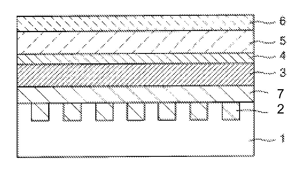
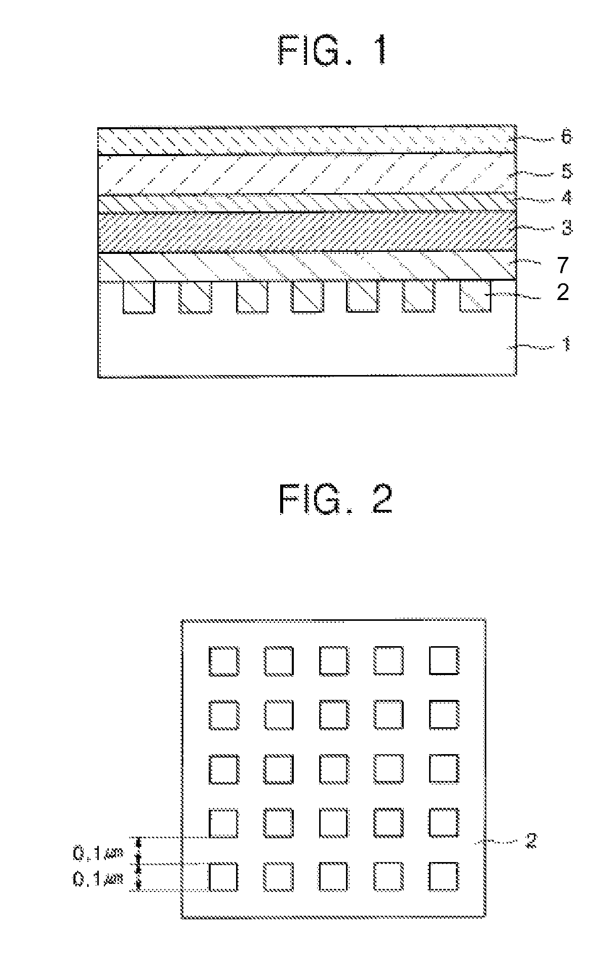
[0049]The structure of Embodiment 1 is shown in FIG. 1. A diffraction grating 2 shown in FIG. 2 was made on a glass substrate of 50 mm×50 mm (NA45 by HOYA, 1.1 mm thick). First, an i-ray resist (THMR-iP1700 by TOKYO OHKA KOGYO CO.) was formed in a thickness of 2 μm on the glass substrate 1 by a spin coating method, and a pattern was formed with a width of 0.1 μm and a space of 0.1 μm using an i-ray stepper. Subsequently, the substrate 1 having the pattern formed therein was immersed in hydrofluoric acid solution and a groove having a depth of 100 nm was formed, and thereafter the remaining resist was eliminated by a dedicated stripper liquid to thus obtain a diffraction grating 2. Subsequently, a Si3N4 film 7 was formed with a thickness of 300 nm by a sputtering method using silicon nitride (Si3N4) as a target. Further, a silicon oxide (SiO2) layer as an intermediate layer 3 was formed in a thickness of 50 nm on the Si3N4 film 7 by the sputtering method, and then an anode 4, an orga...

embodiment 2

[0052]Embodiment 2 is the same as Embodiment 1 except that, in the structure and fabricating process, only the pitch of the diffraction grating 2 was changed to a width of 0.05 μm, a space of 0.05 μm, and a depth of 100 nm.

embodiment 3

[0053]Embodiment 3 is the same as Embodiment 1 except that, in the structure and fabricating process, a glass substrate (NA45 by HOYA, 1.1 mm thick) of 50 mm×50 mm was immersed in standard hydrofluoric acid liquid and the substrate surface was made to be coarse to form a scattering portion.

[0054]Subsequently, this scattering portion was buried, the intermediate layer 3 was formed, and the organic EL layer 5 was formed in the same condition as in Embodiment 1 to fabricate the organic EL device.


PUM


Abstract

The present invention relates to an organic electroluminescent device. There is provided an organic electroluminescent device with a good luminescence property and high luminous efficiency in which the organic electroluminescent device has a diffraction grating 2 on the surface of the substrate 1 and an organic EL layer 5 including an emission layer between an anode 4 an a cathode 6 via an intermediate layer 3.

Description

CROSS-REFERENCE TO RELATED APPLICATION[0001]This application claims the benefit of Japanese Patent Application No. 2003-144769, filed May 22, 2003, the disclosure of which is hereby incorporated herein by reference in its entirety.BACKGROUND OF THE INVENTION[0002]1. Field of the Invention[0003]The present invention relates to an organic electroluminescent device having a good luminescent state and excellent luminous efficiency.[0004]2. Description of the Related Art[0005]The organic electroluminescent device (hereinafter, organic EL device) is an emissive device using a principle in which a fluorescent material emits light using recombination energy of holes injected from an anode and electrons injected from a cathode by electric field application. A representative example of a study on this organic EL device includes a low voltage driving organic EL device using a stacked device, which has been reported by C. W. Tang et al (e.g., see C. W. Tang, S. A. VanSlyke, Applied Physics Lett...

Claims


Application Information

Patent Timeline
Patent Type & Authority Patents(United States)
IPC IPC(8): H05B33/12H05B33/02H01L51/50H01L51/52H05B33/22
CPCH01L51/5262H01L51/5275H01L51/5268H10K50/85H10K50/854H10K50/858H05B33/22
Inventor ONISHI, YASUHARUTOGUCHI, SATORUYAMANARI, JUNICHIISHIKAWA, HITOSHIGOTOH, TOMOHISAKAMIJO, ATSUSHI
Owner SAMSUNG DISPLAY CO LTD
Why Eureka
Try Eureka