Solutions for integrated circuit integration of alternative active area materials

a technology of active area materials and integrated circuits, which is applied in the direction of semiconductor devices, electrical equipment, semiconductor/solid-state device details, etc., to achieve the effects of increasing the functionality and performance of the cmos platform, reducing (a) channel resistance, and high mobility

Active Publication Date: 2009-12-01
TAIWAN SEMICON MFG CO LTD
View PDF222 Cites 122 Cited by
  • Summary
  • Abstract
  • Description
  • Claims
  • Application Information

AI Technical Summary

Benefits of technology

[0004]Heterointegration of alternative materials onto conventional and new substrates is desirable for various electronic and optoelectronic applications. For example, the possibility of the heterointegration of III-V, II-VI materials and/or Ge with Si is an attractive path for increasing the functionality and performance of the CMOS platform. An economical solution to heterointegration could enable new fields of applications, such as replacing Si in CMOS transistors, particularly for critical path logic devices. This could significantly lower (a) channel resistance, due to the ultra-high mobility and saturation velocity afforded by various non-Si semiconductors, and (b) source/drain resis

Problems solved by technology

First, it allows adding the non-Si semiconductor material only where it is needed, a

Method used


Image

  • Solutions for integrated circuit integration of alternative active area materials
  • Solutions for integrated circuit integration of alternative active area materials
  • Solutions for integrated circuit integration of alternative active area materials

Examples


Embodiment Construction

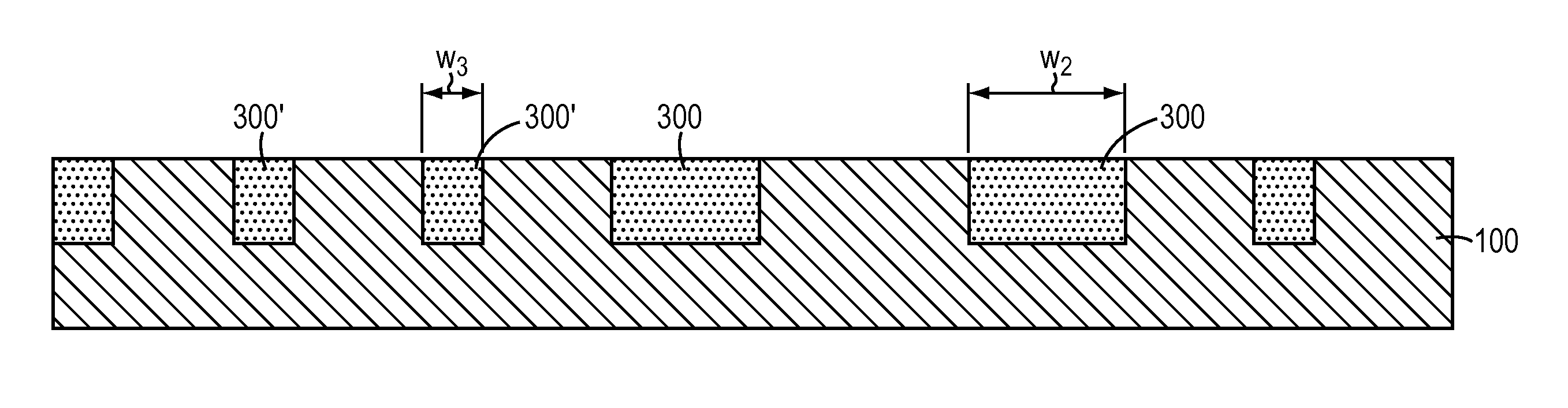
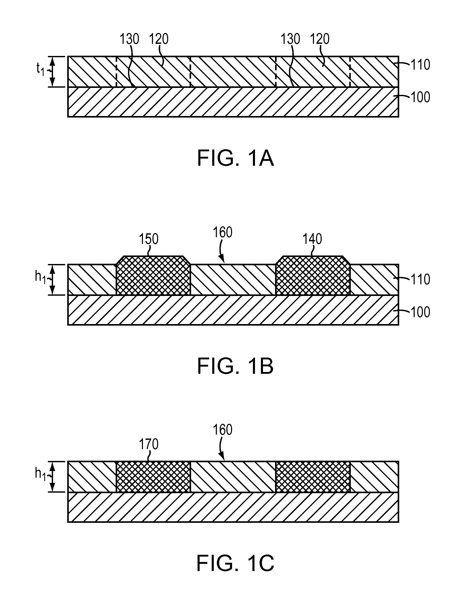
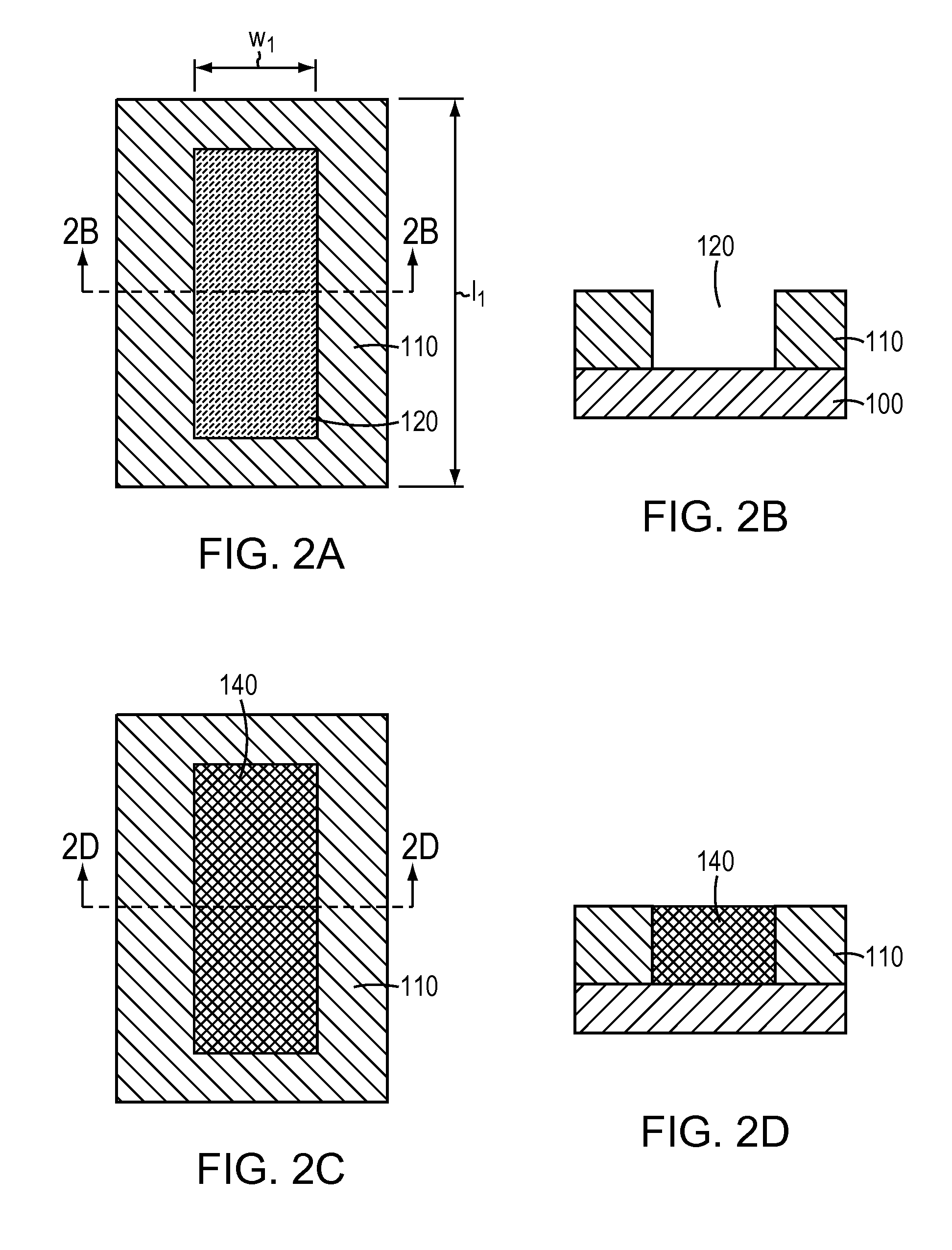
[0042]Referring to FIGS. 1a-1c and 2a-2g, planar isolation regions may be utilized for the selective epitaxy of active area materials. Referring to FIGS. 1a, 2a, and 2b, a substrate 100 includes a crystalline semiconductor material. The substrate 100 may be, for example, a bulk silicon wafer, a bulk germanium wafer, a semiconductor-on-insulator (SOI) substrate, or a strained semiconductor-on-insulator (SSOI) substrate. A masking layer 110 is formed over the substrate 100. The masking layer 110 may be an insulator layer including, for example, silicon dioxide, aluminum oxide, silicon nitride, silicon carbide, or diamond, and may have a thickness t1 of, e.g., 50-1000 nanometers (nm). The masking layer 110 may be formed by a deposition method, such as chemical vapor deposition (CVD), plasma-enhanced chemical vapor deposition (PECVD), low pressure chemical vapor deposition (LPCVD), or a physical deposition method such as sputtering. Alternately, the masking layer 110 may be formed by th...


PUM


Abstract

Methods of forming areas of alternative material on crystalline semiconductor substrates, and structures formed thereby. Such areas of alternative material are suitable for use as active areas in MOSFETs or other electronic or opto-electronic devices.

Description

RELATED APPLICATIONS[0001]This application claims the benefit of U.S. Provisional Application 60 / 702,363 filed Jul. 26, 2005, the entire disclosure of which is hereby incorporated by reference.FIELD OF THE INVENTION[0002]This invention relates to methods and materials for formation of structures including alternative active area materials.BACKGROUND[0003]As geometric scaling of Si-based MOSFET technology becomes more challenging, the heterointegration of alternate materials with Si becomes an attractive option for increasing the innate carrier mobility of MOSFET channels. Heterointegration of alternate materials has thus far been limited to the addition of SiGe alloys of small Ge content for use as source-drain contact materials or heterojunction bipolar transistor base layers. Since such layers are only slightly lattice mismatched to Si, and since most modern Si MOSFET processes are compatible with these dilute SiGe alloys, few disruptions in the Si MOSFET integration sequence have...

Claims


Application Information

Patent Timeline
IPC IPC(8): H01L23/58
CPCH01L21/823807H01L21/823814H01L21/823842H01L21/8258H01L27/0605H01L29/1054H01L29/66636H01L29/7833H01L29/7834H01L29/7848H01L29/165H01L2924/0002H01L2924/00H01L21/8234H01L29/10
Inventor LOCHTEFELD, ANTHONY J.CURRIE, MATTHEW T.CHENG, ZHI-YUANFIORENZA, JAMES
Owner TAIWAN SEMICON MFG CO LTD
Why Eureka
Try Eureka