Conductive paste and multilayer ceramic electronic device and its method of production

a multi-layer ceramic and electronic device technology, applied in the direction of resistive material coating, non-conductive material with dispersed conductive material, fixed capacitors, etc., can solve the problem of ceramic green sheet becoming hard to peel off, ceramic green sheet not becoming a practical problem, and accurately reducing the electrode pattern to a predetermined thickness cannot be obtained, etc. problem, to achieve the effect of easy adsorption of conductive powder, good rheology and low viscosity

Active Publication Date: 2009-12-15
TDK CORPARATION
View PDF20 Cites 2 Cited by
  • Summary
  • Abstract
  • Description
  • Claims
  • Application Information

AI Technical Summary

Benefits of technology

[0026](1) The terpineol acetate used for the solvent of the conductive paste in the present invention sufficiently dissolves the ethyl cellulose generally used for the organic binder of a conductive paste (rheology is good). Therefore, the conductive paste using the present solvent has little change in viscosity along with the elapse of time. The level of solubility can be judged for example by the creep characteristic, tan δ, etc., but the conductive paste of the present invention is superior in the creep characteristic and tan δ (see examples). Therefore, it is believed that the ethyl cellulose contained in the conductive paste as an organic binder is easily adsorbed by the conductive powder and is stable in dispersion and as a result there is less change of viscosity of the conductive paste along with time. By there being less change in viscosity over time, it is possible to suppress the change in thickness along with time at the time of formation of the electrodes.
[0027]Note that the creep characteristic and the tan δ both become indicators for judgment of the solubility. If dropping paste of a certain viscosity on a base material etc., the paste dropped on the base material naturally tends to become flat (to become level). The creep characteristic is an indicator showing the ease of leveling of this paste. If the creep characteristic is good, it means that the leveling ability is superior and it is believed that in turn the solubility is high (dissolves well). The inventors discovered that the terpineol acetate used in the present invention is much more superior in creep characteristic compared with terpineol, dihydroterpineol, dihydroterpineol acetate, etc. (see FIG. 2).
[0028]The tan δ is an indicator for judging the dynamic viscoelasticity. The lower the tan δ value, the more elastic and the harder the leveling. On the other hand, the higher the tan δ value, the less elastic and the easier the leveling. The larger the tan δ, the better the dynamic viscoelasticity, that is, the better the leveling ability and in turn the higher the solubility. The inventors discovered that the terpineol acetate used in the present invention has a higher and better tan δ compared with the nonsoluble dihydroterpineol or dihydroterpineol acetate other than terpineol (see FIG. 3).
[0029](2) Further, the terpineol acetate used for the solvent of the conductive paste in the present invention does not cause the butyral resin contained as an organic binder in the ceramic green sheet to dissolve or swell (nonsoluble). Therefore, the conductive paste used in the present solvent, while secondarily, also has the effect of preventing sheet attack. Therefore, even if the thickness of the ceramic green sheet is for example a thin one of 5 μm or less, when printing the conductive paste, then peeling off the ceramic green sheet from a PET film or other carrier sheet, the peelability of the ceramic green sheet is improved and the ceramic green sheet wrinkling, being punctured, cracking, etc. can be effectively suppressed. That is, even if making the ceramic green sheet even thinner than now, no sheet attack phenomenon will occur. As a result, a normal stack is obtained even if using ceramic green sheets of extremely thin thicknesses of 5 μm or less and the finally obtained multilayer ceramic electronic device is no longer liable to suffer from short-circuit defects, withstand voltage defects (IR deterioration), or delamination between the dielectric layers and the internal electrode layers. From the above (1) and (2), the conductive paste of the present invention is extremely advantageous for reducing the size and raising the capacity of the finally obtained multilayer ceramic electronic device.
[0030]That is, according to the present invention, there are provided a conductive paste used for forming internal electrodes of a multilayer ceramic electronic device, with little change in viscosity along with the elapse of time, and free from sheet attack, a multilayer ceramic electronic device produced using the paste, and method of production of that device.
[0031]The multilayer ceramic electronic device is not particularly limited, but a multilayer ceramic capacitor, multilayer ceramic inductor, multilayer ceramic LC device, multilayer ceramic board, etc. may be illustrated.

Problems solved by technology

However, if printing a conductive paste using terpineol as a solvent on a ceramic green sheet, the problem of seepage etc. occurred and electrode patterns accurately reduced to a predetermined thickness cannot be obtained.
This sheet attack phenomenon does not become a practical problem while the ceramic green sheet is relatively thick.
However, when the thickness of a ceramic green sheet is for example 5 μm or less, if the sheet attack phenomenon occurs, when printing the conductive paste, then peeling off the ceramic green sheet from a polyethylene terephthalate (PET) film or other carrier sheet, the ceramic green sheet becomes hard to peel off.
If the ceramic green sheet becomes hard to peel off, this results in the ceramic green sheet wrinkling, being punctured, cracking, etc. and makes it impossible to obtain a normal stack in the stacking process.
If a normal stack cannot be obtained, the finally obtained multilayer ceramic electronic device suffers from short-circuit defects, withstand voltage defects (IR deterioration), and the phenomenon of peeling between the dielectric layers and internal electrode layers (delamination) which in turn cause a drop in yield.
However, the conductive pastes described in Japanese Patent Publication (A) No. 9-17687 and Japanese Patent No. 2976268 using dihydroterpineol or dihydroterpineol acetate as a solvent have the problem of a tendency to increase in viscosity along with time.
Therefore, while the viscosity is as desired and the pastes can be formed on ceramic green sheets to a predetermined thickness at the start of printing, after the elapse of a predetermined time, the viscosity increases and the same thickness cannot be formed under the printing conditions of the start of printing.
This problem tends to manifest itself when desiring to form the electrode patterns particularly thin.
Therefore, with such conventional conductive pastes, there were limits to the reduction of size and increase in capacity of multilayer ceramic electronic devices.

Method used


Image

  • Conductive paste and multilayer ceramic electronic device and its method of production
  • Conductive paste and multilayer ceramic electronic device and its method of production
  • Conductive paste and multilayer ceramic electronic device and its method of production

Examples


embodiment

Actions and Effects of Embodiment

[0081]In the present embodiment, terpineol acetate is used as the solvent of the conductive paste. Therefore, there is less change in viscosity of the conductive paste along with time and the change in thickness along with time at the time of electrode formation can be suppressed.

[0082]Further, in this embodiment, the terpineol acetate used for the solvent of the conductive paste does not cause the polyvinyl butyral contained as an organic binder in the ceramic green sheet to swell or dissolve. That is, it does not cause sheet attack, so even if the thickness of the ceramic green sheets is for example a thin 5 μm or less, when printing the conductive paste, then peeling off the ceramic green sheets from the carrier sheets, the peelability of the ceramic green sheets is improved and the ceramic green sheets wrinkling, being punctured, cracking, etc. can be effectively suppressed. That is, even if the ceramic green sheets are made thinner than ever bef...

example 1

Preparation of Organic Vehicle

[0087]The ethyl cellulose used as the organic binder and the solvent shown in Table 1 were prepared.

[0088]Next, 10 parts by weight of the organic binder was made to dissolve in 100 parts by weight of the solvent to prepare an organic vehicle.

[0089]Evaluation of Creep Characteristic and Tan δ

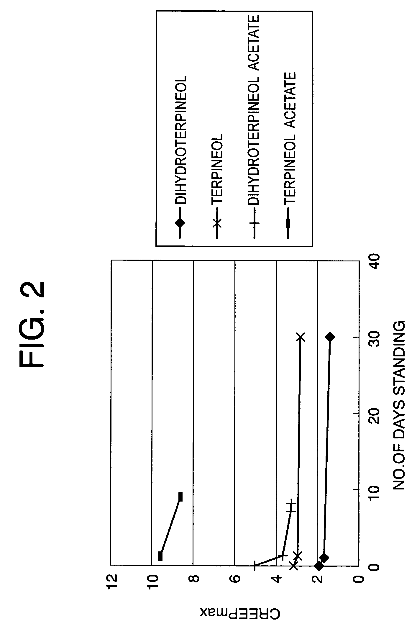
[0090]The “creep characteristic” and “tan δ” of the obtained organic vehicle were evaluated by observing their fluctuation.

[0091]For the “creep characteristic (creep measurement)”, the fluctuation in the maximum creep value when applying a stress of 1 Pa to the obtained organic vehicle was measured by a viscosity / viscoelasticity measurement system (Rheostress RS1, made by Eiko Seiki). The results are shown in FIG. 2. The larger the value of the maximum creep (displacement) with respect to the number of days of standing, the better the creep characteristic, that is, the better the leveling ability, and the higher the solubility (the better the dissolution), it is beli...

example 2

Preparation of Dielectric Paste

[0100]A BaTiO3-based ceramic powder, polyvinyl butyral (PVB) for use as an organic binder, and methanol for use as a solvent were prepared. Next, with respect to the ceramic powder, 10 wt % of an organic binder and 150 wt % of a solvent were weighed and kneaded by a ball mill to form a slurry and obtain a dielectric paste.

[0101]Preparation of Test Samples

[0102]PET films were coated with the above dielectric paste by the doctor blade method to a predetermined thickness and dried to form ceramic green sheets with a thickness of 1 μm. Next, the obtained ceramic green sheets were formed with conductive paste containing the terpineol acetate used in Example 1 by the screen printing method in predetermined patterns to obtain ceramic green sheets with electrode patterns of a thickness about 1.0 μm (test samples).

[0103]Evaluation of Test Samples

[0104]The obtained test samples were used to evaluate the “presence of sheet attack” and the “peelability of the PET ...


PUM

PropertyMeasurementUnit
thicknessaaaaaaaaaa
thicknessesaaaaaaaaaa
thicknessaaaaaaaaaa

Abstract

A conductive paste used for forming internal electrodes of a multilayer ceramic electronic device, used in combination with ceramic green sheets, each containing a butyral resin and having a thickness of 5 μm or less, and including a conductive powder and an organic vehicle, a solvent in said organic vehicle having terpineol acetate as its main ingredient, whereby there is little change in viscosity along with time and no occurrence of sheet attack.

Description

BACKGROUND OF THE INVENTION[0001]1. Field of the Invention[0002]The present invention relates to a conductive paste used for forming internal electrodes of a multilayer ceramic electronic device, a multilayer ceramic electronic device produced using that paste, and a method of production of the device.[0003]2. Description of the Related Art[0004]In recent years, electronic apparatuses have been made thinner and smaller. Along with this, the multilayer ceramic electronic devices used for these electronic apparatuses are also being made smaller in size and higher in capacity.[0005]The most effective method for reducing the size and increasing the capacity of a multilayer ceramic capacitor, explained here as an example of a multilayer ceramic electronic device, is to make both the internal electrodes and dielectric layers as thin as possible and stack as many of them as possible.[0006]A multilayer ceramic capacitor is produced by printing ceramic green sheets having a ceramic powder su...

Claims


Application Information

Patent Timeline
Patent Type & Authority Patents(United States)
IPC IPC(8): H01G4/12H01B1/22
CPCH01B1/22H01G4/30H01G4/0085H05K1/092H01G4/008H01G4/232H01G4/12
Inventor ODA, KAZUHIKOMARUNO, TETSUJIMIURA, SHUICHITAKAHASHI, MAKOTOKOJIMA, TATSUYA
Owner TDK CORPARATION
Why Eureka
Try Eureka