
N-type semiconductor materials in thin film transistors and electronic devices

a technology of thin film transistors and semiconductor materials, applied in the direction of naphthalimide/phthalimide dyes, transportation and packaging, synthetic resin layered products, etc., can solve the problems of amorphous silicon, amorphous silicon still has its drawbacks, and limited application of amorphous silicon to relatively low speed devices

Inactive Publication Date: 2010-01-19
EASTMAN KODAK CO
View PDF13 Cites 15 Cited by
  • Summary
  • Abstract
  • Description
  • Claims
  • Application Information

AI Technical Summary

Benefits of technology

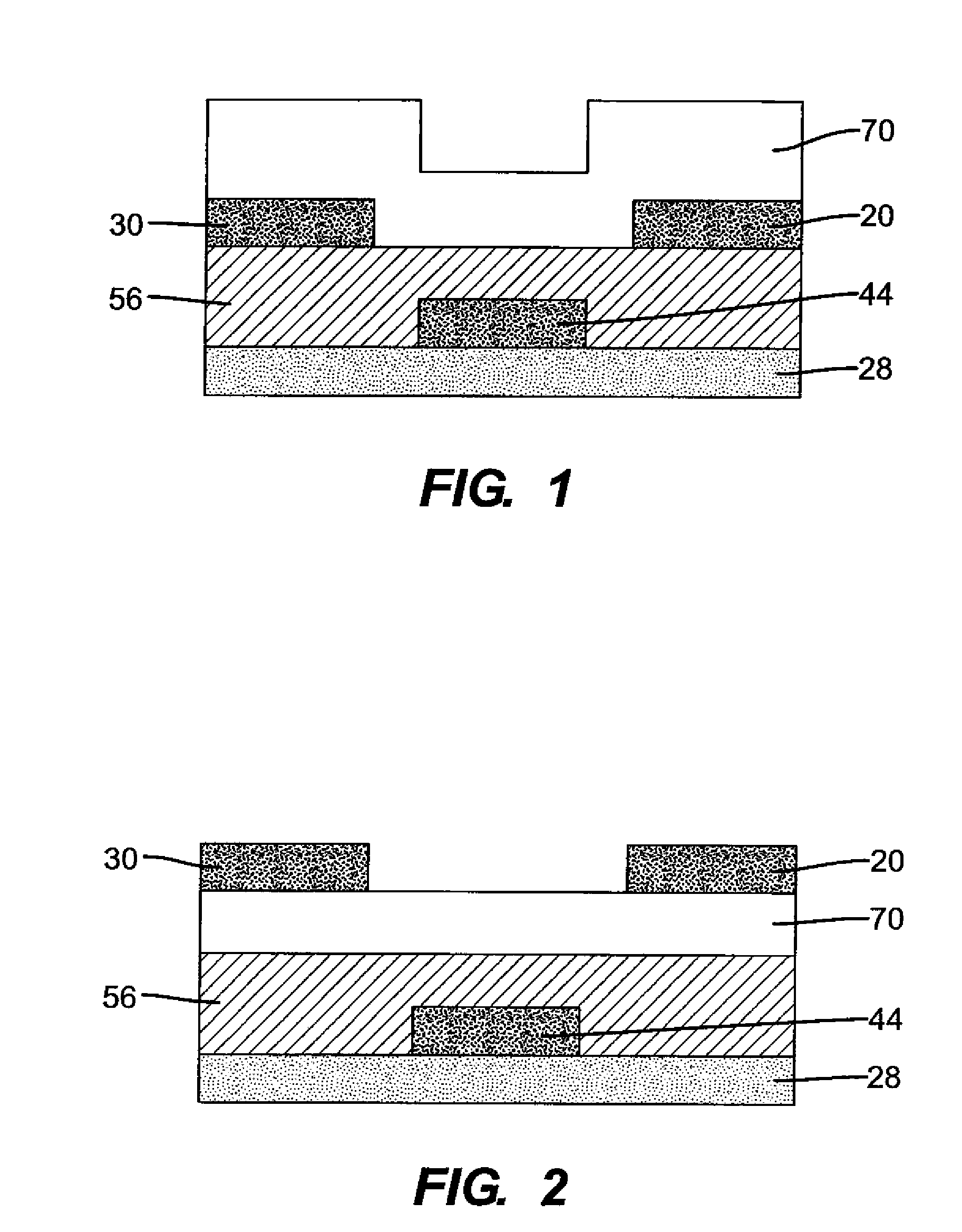
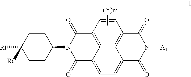
The present invention provides an article comprising a thin film transistor that includes a thin film of organic semiconductor material that contains a specific naphthalene tetracarboxylic acid diimide compound with a fluorinated substituent. This compound exhibits improved operational effectiveness and stability compared to other similar compounds. The thin film transistor has a high field effect electron mobility and can provide high device on / off ratios. The invention also provides an electronic device that includes this thin film transistor and a process for fabricating the thin film transistor. The technical effects of this invention include improved performance and stability of organic thin film transistors and improved efficiency of electronic devices that use them.

Problems solved by technology

Application of amorphous silicon is limited to relatively low speed devices, however, since its maximum mobility (0.5-1.0 cm2 / V sec) is about a thousand times smaller than that of crystalline silicon.
Although amorphous silicon is less expensive than highly crystalline silicon for use in TFT's, amorphous silicon still has its drawbacks.
The deposition of amorphous silicon, during the manufacture of transistors, requires relatively costly processes, such as plasma enhanced chemical vapor deposition and high temperatures (about 360° C.) to achieve the electrical characteristics sufficient for display applications.
Such high processing temperatures disallow the use of substrates for deposition that are made of certain plastics that might otherwise be desirable for use in applications such as flexible displays.
One such material, buckminsterfullerene C60, exhibits a mobility of 0.08 cm2 / Vs but is considered unstable in air.
One such naphthalene-based n-channel semiconductor material, tetracyanonaphthoquino-dimethane (TCNNQD), is capable of operation in air, but the material has displayed a low on / off ratio and is also difficult to prepare and purify.
However, Marks et al. do not see any comparative advantage of using cycloalkyl groups on the imide nitrogens.
In practice the preparation of very pure cis or trans-1,4-substituted cyclohexanes can be problematic, and often mixtures, to some extent, of cis and trans substituted compounds are prepared.

Method used


Image

  • N-type semiconductor materials in thin film transistors and electronic devices
  • N-type semiconductor materials in thin film transistors and electronic devices
  • N-type semiconductor materials in thin film transistors and electronic devices

Examples


invention example 1

[0133]The purified configurationally controlled N,N′-(trans-4-trifluoromethylcyclohexyl)-1,4,5,8-naphthalene tetracarboxylic acid diimide I-2 was deposited by vacuum sublimation at a pressure of 2×10⁻⁷ Torr and a rate of 0.1 Angstroms per second to a thickness of 17-20 nm as measured by a quartz crystal. During deposition the substrate was held at room temperature of 20° C. The sample was exposed to air for a short time prior to subsequent deposition of Au source and drain electrodes through a shadow mask to a thickness of 50-60 nm. The devices made had a 600 μm channel width, with channel lengths varying from 50 to 150 μm. Multiple OTFTs were prepared and representative samples of 4 to 8 OTFTs were tested for each deposition run. Devices were tested both under argon (Ar) and in air. The averaged results appear in TABLE I below.

[0134]

TABLE IActiveOTFTTestμVthMaterialConditions(cm2 / Vs)σ (μ)(V)σ (Vth)IonIoffComparativeC-1Under argon0.330.0439.173.551.34 × 107Example 1Air0.350.0263.33....

invention example 2

[0137]A heavily doped silicon wafer with a thermally-grown SiO2 layer with a thickness of 185 nm was used as the substrate. The wafer was cleaned for 10 minutes in a piranha solution, followed by a 6-minute exposure in a UV / ozone chamber. The purified I-2 was deposited by vacuum sublimation at a pressure of 2×10⁻⁷ Torr and a rate of 0.1 Angstroms per second to a thickness of 17-20 nm as measured by a quartz crystal. During deposition the substrate was held at room temperature of 20° C. The sample was exposed to air for a short time prior to subsequent deposition of Au source and drain electrodes through a shadow mask to a thickness of 50 nm. The devices made had a 600 μm channel width, with channel lengths varying from 50 to 150 μm. Multiple OTFT's were prepared and representative samples of 4 to 8 OTFT's were tested for each deposition run. Devices were tested in air. The averaged results appear in TABLE II below.

[0138]

TABLE IIActiveOTFTTestμVthMaterialConditions(cm2 / Vs)σ (μ)(V)σ (...

invention example 3

[0140]This example demonstrates the improved performance of an n-type TFT device using N,N′-(cis-4-trifluoromethylcyclohexyl)-1,4,5,8-naphthalene tetracarboxylic acid diimide (Compound I-3) in accordance with the present invention. An n-type OTFT device comprising Compound I-3 as the active material was made as described earlier in Invention Example 1. The averaged results appear in TABLE III below.

[0141]

TABLE IIIActiveOTFTTestμVthMaterialConditions(cm2 / Vs)σ (μ)(V)σ (Vth)IonIoffComparativeC-1Under Ar0.330.0439.173.551.34 × 107Example 1Air0.350.0263.33.542.57 × 107InventiveI-3Under Ar0.190.0120.433.673.44 × 107Example 3Air0.200.0320.211.627.55 × 106

[0142]Comparative Example 1 and Invention Example 3 clearly demonstrate the advantage of using Compound I-3 as n-type material in a thin film transistor. The Vth position of the invention device was improved over Comparative Example 1 demonstrating the advantageous effect on device performance of fluoroalkyl group substituted cyclohexane r...


PUM

PropertyMeasurementUnit
temperatureaaaaaaaaaa
temperaturesaaaaaaaaaa
drain-source voltageaaaaaaaaaa

Abstract

A thin film transistor comprises a layer of organic semiconductor that comprises an N,N′-1,4,5,8-naphthalenetetracarboxylic acid diimide having at least one cycloalkyl group having a fluorinated substituent at its 4-position that adopts an equatorial orientation in the trans configuration of the cycloalkyl group and an axial orientation in the cis configuration of the cycloalkyl group. Such transistors can be a field effect transistor having a dielectric layer, a gate electrode, a source electrode and a drain electrode. The gate electrode and the thin film of organic semiconductor material both contact the dielectric layer, and the source electrode and the drain electrode both contact the thin film of organic semiconductor material.

Description

FIELD OF THE INVENTION[0001]The present invention relates to the use of N,N′-1,4,5,8-naphthalenetetracarboxylic acid diimides having a fluorinated cycloalkyl substituent as semiconductor materials in n-channel semiconductor films for thin film transistors. The invention also relates to the use of these materials in thin film transistors for electronic devices and methods of making such transistors and devices.BACKGROUND OF THE INVENTION[0002]Thin film transistors (TFT's) are widely used as switching elements in electronics, for example, in active-matrix liquid-crystal displays, smart cards, and a variety of other electronic devices and components thereof. The thin film transistor (TFT) is an example of a field effect transistor (FET). The best-known example of an FET is the MOSFET (Metal-Oxide-Semiconductor-FET), today's conventional switching element for high-speed applications. Presently, most thin film devices are made using amorphous silicon as the semiconductor. Amorphous silic...

Claims


Application Information

Patent Timeline
Patent Type & Authority Patents(United States)
IPC IPC(8): H01L51/00C07D471/02H10K99/00
CPCC07D471/06H01L51/0053Y02E10/549H01L51/42H01L51/0545Y10T428/31721C09B57/08H10K85/621H10K10/466H10K30/00
Inventor SHUKLA, DEEPAKWELTER, THOMAS R.
Owner EASTMAN KODAK CO
Learn More