

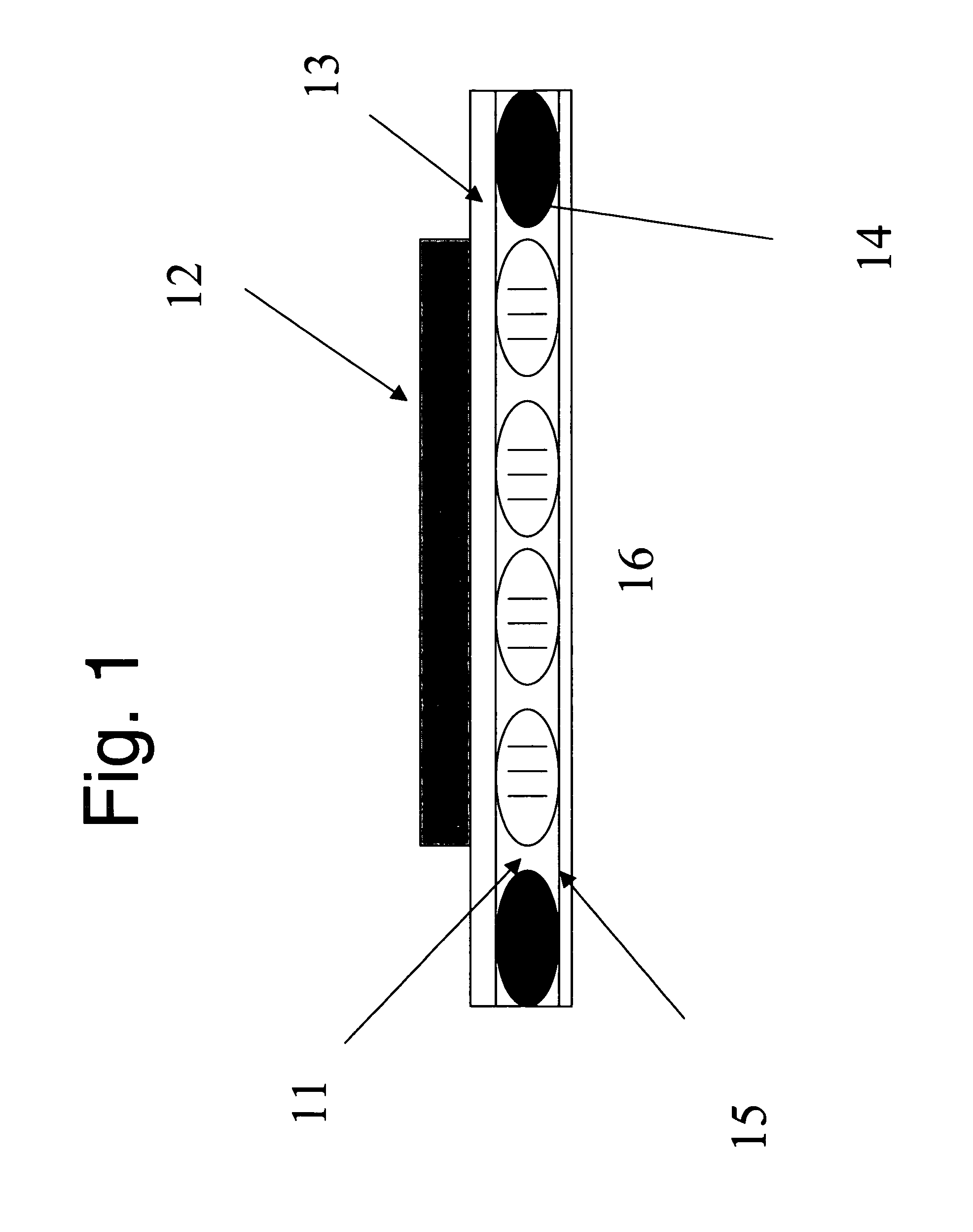
Single substrate guest-host polymer dispersed liquid crystal displays
a polymer dispersed liquid crystal display and single substrate technology, applied in the direction of photosensitive materials, instruments, photomechanical equipment, etc., can solve the problems of loss of performance, uv radiation is harmful to liquid crystals, change in reflected color, etc., to achieve low switching voltage, good contrast, and low cost
- Summary
- Abstract
- Description
- Claims
- Application Information
AI Technical Summary
Benefits of technology
Problems solved by technology
Method used
Image

Examples
example 1
Invention
[0103]This example shows fabrication and evaluation of a guest-host PDLC display by the method of our invention.
[0104]The dichroic dye Blue AB4 from Nematel, Germany was combined with the nematic host mixture BL087 from Merck to prepare a guest-host liquid crystal composition containing 1 wt % dichroic dye
[0105]A dispersion of the guest-host liquid crystal composition was prepared as follows. To 241 grams of distilled water was added 3.6 grams of Ludox™ colloidal silica suspension and 7.4 grams of a 10% w / w aqueous solution of a copolymer of methylaminoethanol and adipic acid. To this was added 108 grams of the guest-host liquid crystal composition. The mixture was stirred using a Silverson mixer at 5000 rpm. It was then passed through a microfluidizer at 3000 psi. Finally, the resulting dispersion was passed through a 23 μm filter. The droplet size distribution in the dispersion was measured using a Coulter Counter. It was found that the mean size was 9.7 microns with a co...
example 2
Control
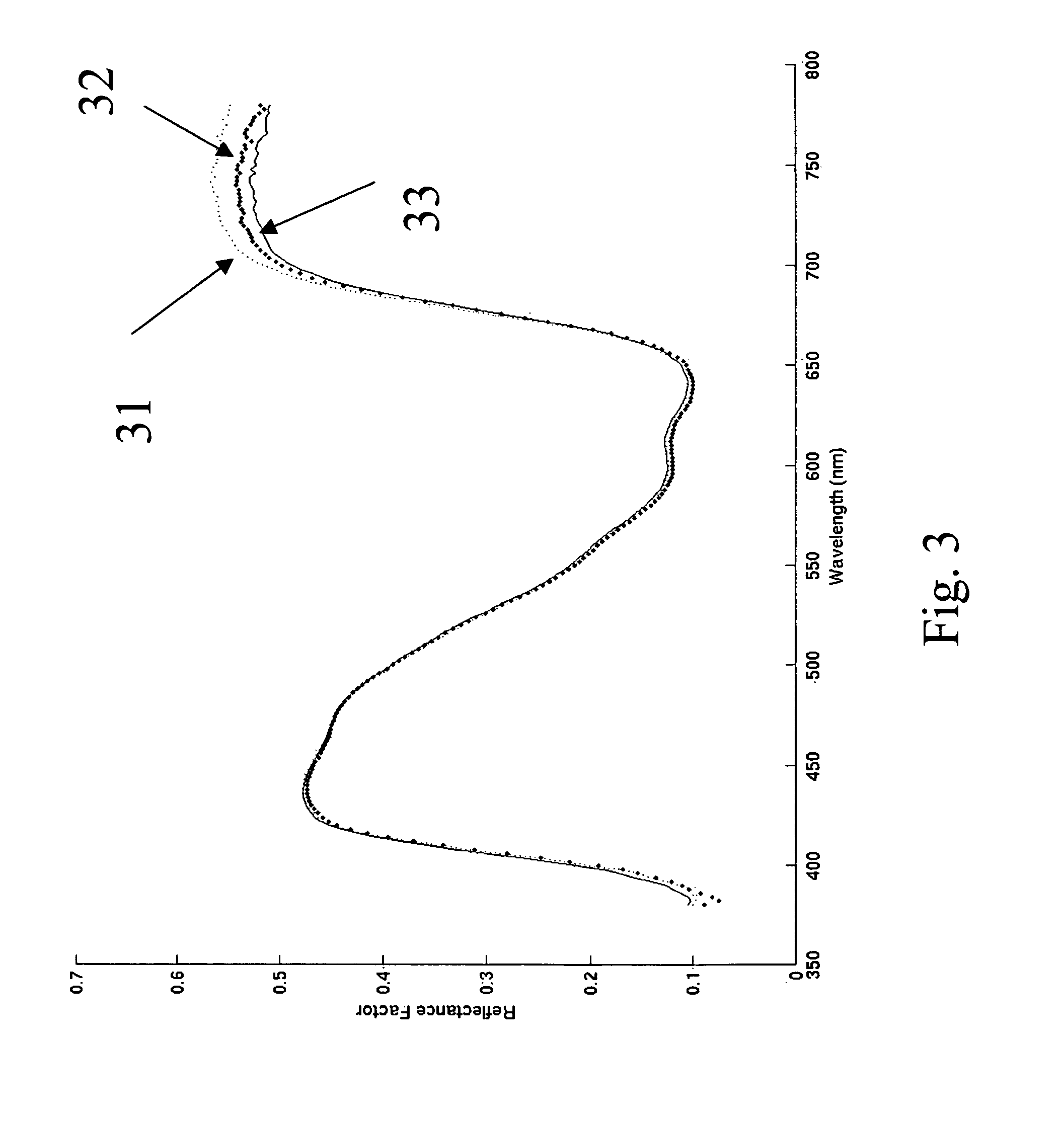
[0110]This example shows fabrication and evaluation of a cholesteric or chiral nematic PDLC display.
[0111]A chiral nematic liquid crystal (CLC) composition with wavelength of reflection centered around 550 nm was prepared by adding an appropriate amount of high twist chiral dopant to the nematic host BL087 (from Merck).
[0112]A dispersion of the CLC composition was prepared and coated in a manner similar to that described for the guest-host liquid crystal material in Example 1 except that a dispersion of carbon black was used as contrast control agent in the overcoat layer in place of titania.
[0113]FIG. 4 shows the reflectance spectra of the green reflecting state of the sample at different viewing angles of 45 degrees 41, 60 degrees 42 and viewing angle 22.5 degrees 43 measured using the same apparatus described in Example 1. In this case there is a noticeable shift in the reflectance spectrum to lower wavelengths at higher viewing angles resulting in an overall appearance th...
PUM
| Property | Measurement | Unit |
|---|---|---|
| thickness | aaaaa | aaaaa |
| domain size | aaaaa | aaaaa |
| particle size | aaaaa | aaaaa |
Abstract
Description
Claims
Application Information