Semiconductor element and electrical apparatus

a technology of semiconductors and elements, applied in the direction of dynamo-electric converter control, semiconductor/solid-state device details, dynamo-electric gear control, etc., can solve the problems of increasing switching loss, reducing power use efficiency, and large entire switching loss, and achieves high-speed switching operation and energy loss reduction, and excels in resistance to current concentration. , the effect of suppressing the breaking of an end portion

Active Publication Date: 2010-09-07
PANASONIC CORP
View PDF33 Cites 14 Cited by
  • Summary
  • Abstract
  • Description
  • Claims
  • Application Information

AI Technical Summary

Benefits of technology

[0039]The present invention can provide a semiconductor element and an electrical apparatus each of which can realize both high-speed switching operation and energy loss reduction, excels in resistance to current concentration based on the counter electromotive voltage generated by, for example, the inductance load of the electrical apparatus, and suppresses breaking of an end portion of the element.

Problems solved by technology

Moreover, since this current becomes a loss current, the switching loss increases, and the power use efficiency decreases.
Thus the entire switching loss becomes large.
However, in the case of using the IGBT as the switching element, since the IGBT is a bipolar device, the lifetime of the minority carrier is long, and the time required for the reverse recovery is long.
However, in the case of the MOSFET made of silicon, the ON-resistance Ron (Ωcm2) per unit area is high, and a conduction loss due to heat generation increases.
However, it is difficult for the fast recovery diode to operate at a high frequency of several tens of kHz or more.
However, since the schottky diode made of silicon has the withstand voltage of only about 100 V, it cannot be used in a power electronics field which requires the withstand voltage of 600 V or higher.
Moreover, since the IGBT and diode made of silicon are subjected to the carrier lifetime control, they cannot be integrated in one chip.
However, even in the case of a SiC-MISFET, by a parasitic diode constituted of a PN junction of a p-type region and an n-type region in a semiconductor device, a reverse recovery time delay may occur in the case of switching from an ON state of the parasitic diode to an OFF state of the SiC-MISFET when a reverse bias is applied.
For example, when a positive voltage that is a counter electromotive voltage generated by an inductance load when the switching element is turned OFF is applied to a source electrode, positive holes as minority carriers are implanted in the n-type region via the parasitic diode, and this causes the reverse recovery time delay of the operation of the parasitic diode.

Method used


Image

  • Semiconductor element and electrical apparatus
  • Semiconductor element and electrical apparatus
  • Semiconductor element and electrical apparatus

Examples


embodiment 1

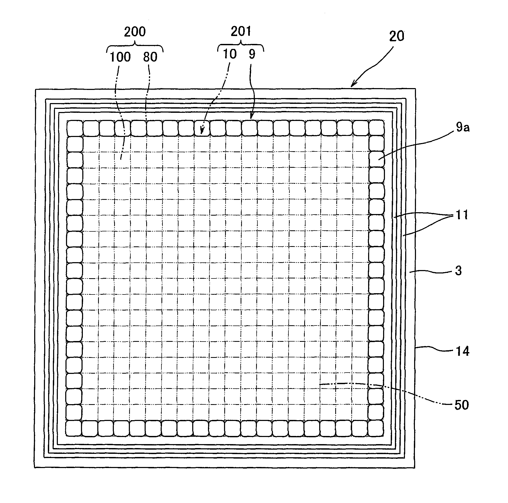
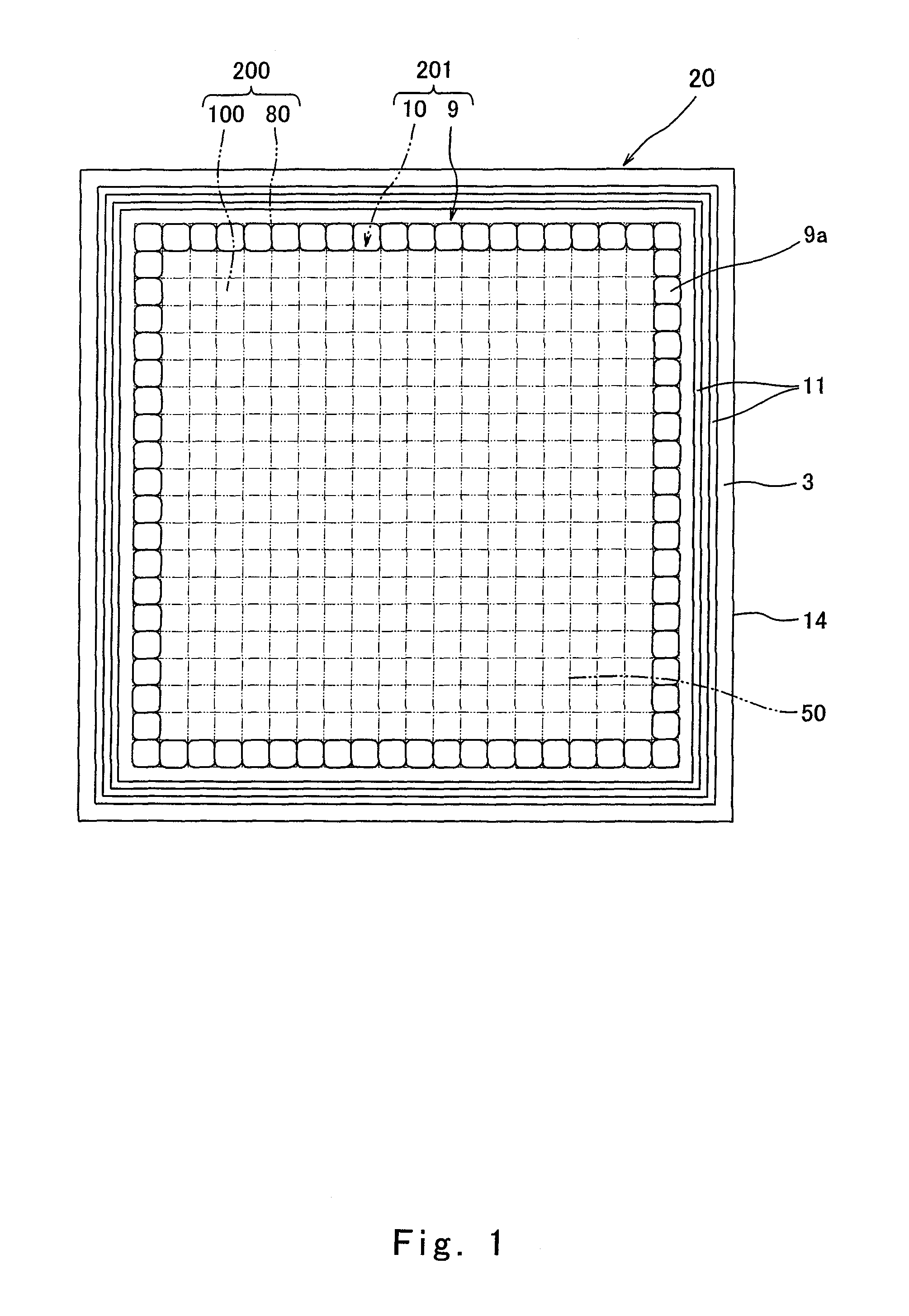
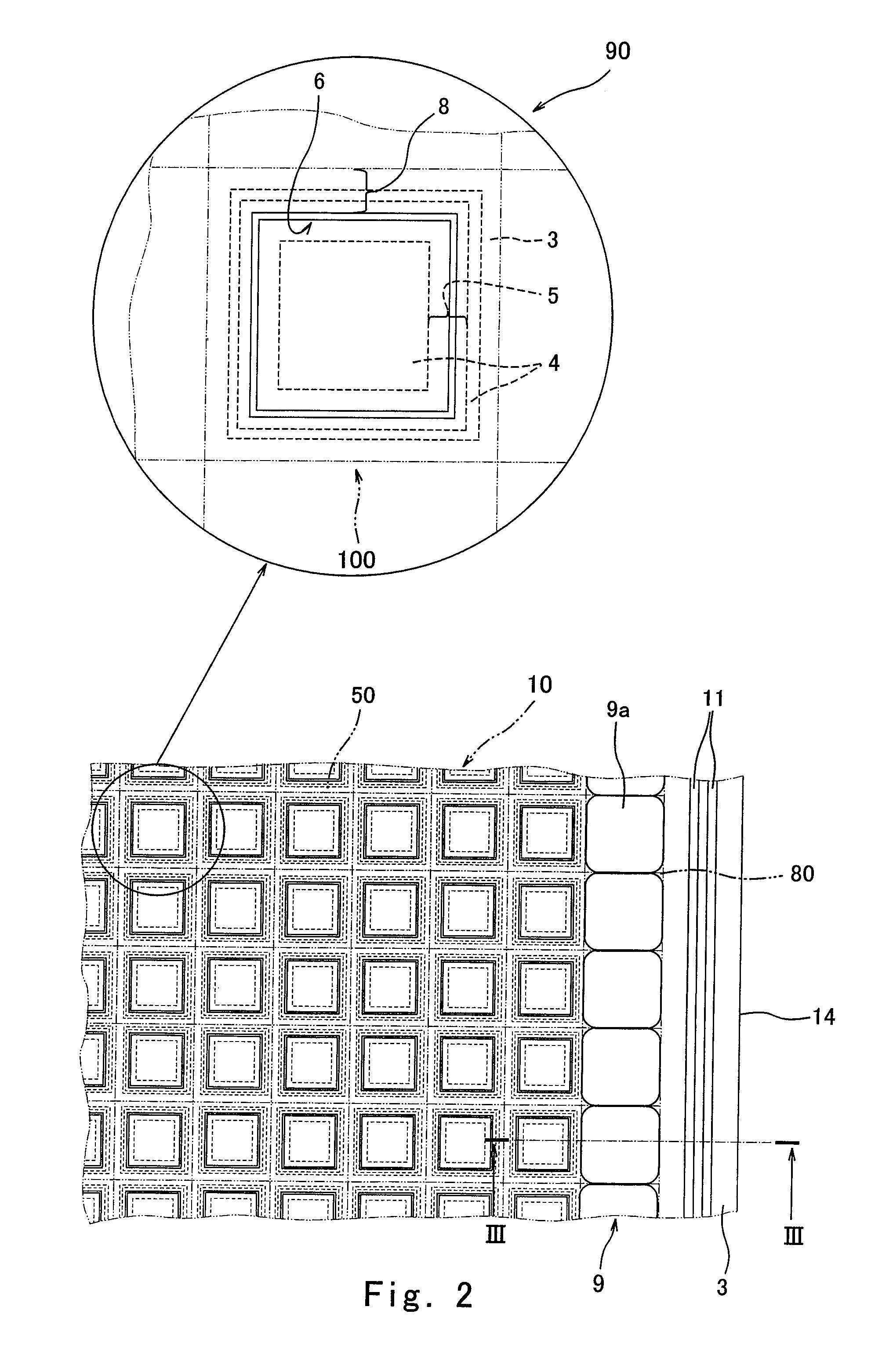
[0097]FIG. 1 is a plan view showing the construction of a semiconductor element of Embodiment 1 of the present invention. FIG. 2 is a partial plan view enlarging part of the construction of the semiconductor element of FIG. 1. FIG. 3 is a partial cross-sectional view showing the construction of the semiconductor element of FIG. 1 in cross section, and is a cross-sectional view taken along line III-III of FIG. 2.

[0098]A semiconductor element of the present embodiment functions as a circuit in which a field effect transistor (hereinafter may be referred to as “MOSFET”) and a schottky diode are connected in parallel to each other, and is constituted of one IC chip in which a plurality of field effect transistors and a plurality of schottky diodes constituting the above circuit are integrated. For example, the semiconductor element of the present embodiment is used as a phase switching circuit 23 in an inverter circuit (see FIG. 5) for driving a three-phase motor. The number of field ef...

embodiment 2

[0177]Embodiment 2 of the present invention exemplifies an inverter circuit which incorporates therein an arm module (semiconductor device) using the semiconductor element 20 of Embodiment 1.

[0178]Arm Module

[0179]FIG. 4 is a plan view schematically showing the construction of the arm module as the semiconductor device according to Embodiment 2 of the present invention. In FIG. 4, the same reference numbers as in FIGS. 1 to 3 are used for the same or corresponding members, and explanations thereof are omitted.

[0180]As shown in FIG. 4, the arm module of the present embodiment includes the semiconductor element 20 of Embodiment 1 and a package having a drain electrode terminal 15, a source electrode terminal 16 and a gate electrode terminal 17.

[0181]The semiconductor element 20 is disposed on the drain electrode terminal 1 such that the drain electrode 1 is connected to an upper surface of the drain electrode terminal 15. The source schottky pads 12S of the semiconductor element 20 are...

embodiment 3

[0201]FIG. 6 is a plan view showing the construction of a semiconductor element of Embodiment 3 of the present invention. FIG. 7 is a partial plan view enlarging part of the construction of the semiconductor element of FIG. 6. In FIGS. 6 and 7, the same reference numbers as in FIGS. 1 and 2 are used for the same or corresponding members, and explanations thereof are omitted.

[0202]As shown in FIGS. 6 and 7, in the semiconductor element 20 of the present embodiment, the diode forming region 9 is constructed such that the schottky electrodes 9b which cover the upper surfaces of a plurality of diode cells 80 among the cells 200 defined by the lattice-like virtual border lines 50 in plan view are disposed so as to surround the outer periphery of the transistor forming region 10. Other than this point, the semiconductor element 20 of Embodiment 3 is the same as that of Embodiment 1.

[0203]Four schottky electrodes 9b are disposed so as to extend along the outer periphery of the transistor f...


PUM


Abstract

A semiconductor element (20) of the present invention includes a plurality of field effect transistors (90) and a schottky electrode (9a), and the schottky electrode (9a) is formed along an outer periphery of a region where the plurality of field effect transistors (90) are formed.

Description

RELATED APPLICATIONS[0001]This application is the U.S. National Phase under 35 U.S.C. §371 of International Application No. PCT / JP2006 / 314489, filed on Jul. 21, 2006, which in turn claims the benefit of Japanese Application No. 2005-214196, filed on Jul. 25, 2005, the disclosures of which Applications are incorporated by reference herein.TECHNICAL FIELD[0002]The present invention relates to a semiconductor element, and particularly to a semiconductor power switching element which controls an inverter circuit, etc.BACKGROUND ART[0003]One example of a normal semiconductor power switching element is an IGBT (Insulated Gate Bipolar Transistor). One application example of the semiconductor power switching element is a control circuit for use in power electronics control, such as an inverter circuit which controls a three-phase motor.[0004]FIG. 8 is a circuit diagram schematically showing this conventional inverter circuit. As shown in FIG. 8, the conventional inverter circuit (three-phas...

Claims


Application Information

Patent Timeline
Patent Type & Authority Patents(United States)
IPC IPC(8): H02P21/04H02M3/335H01L29/772H01L29/06H01L29/12H01L29/78H01L29/872H02M7/48
CPCH01L23/62H01L24/06H01L24/48H01L24/49H01L27/0629H01L29/0696H01L29/66068H01L29/7806H01L29/7811H01L2924/01042H01L2924/01079H01L2924/01082H01L2924/13055H01L2924/13091H01L2924/14H01L2924/19042H01L2924/19043H01L2924/30107H01L29/0619H01L29/1602H01L29/1608H01L29/2003H01L29/47H01L2224/04042H01L2224/05624H01L2224/05644H01L2224/05655H01L2224/05666H01L2224/0568H01L2224/45124H01L2224/45144H01L2224/48091H01L2224/4813H01L2224/48247H01L2224/48472H01L2224/4903H01L2224/49051H01L2224/4911H01L2224/49175H01L2224/85424H01L2224/85444H01L2924/01004H01L2924/01005H01L2924/01007H01L2924/01013H01L2924/01014H01L2924/01015H01L2924/01018H01L2924/01022H01L2924/01025H01L2924/01027H01L2924/01028H01L2924/01033H01L2924/01006H01L2924/01023H01L2224/4868H01L2224/48724H01L2224/48755H01L2224/48766H01L2224/4878H01L2224/48624H01L2224/48644H01L2224/48655H01L2224/48666H01L2224/05554H01L2924/1306H01L2924/12032H01L2924/1305H01L2224/0603H01L2924/00014H01L2924/00H01L2224/48744H01L2224/45015H01L2924/12036H01L2924/12041H01L2224/85399H01L24/45
Inventor KITABATAKE, MAKOTOKUSUMOTO, OSAMUUCHIDA, MASAOYAMASHITA, KENYA
Owner PANASONIC CORP
Why Eureka
Try Eureka