Gallium nitride based compound semiconductor device including compliant substrate and method for manufacturing the same

a gallium nitride and semiconductor technology, applied in the direction of polycrystalline material growth, crystal growth process, chemically reactive gas growth, etc., can solve the problems of significantly prolonged run time of the mocvd reactor necessary for fabricating the device, inability to estimate the buffer layer during the growth thereof, and prolonged time required for the mocvd process. achieve the effect of reducing the total process time of the mocvd process and high quality

Inactive Publication Date: 2010-09-14
THELEDS
View PDF4 Cites 1 Cited by
  • Summary
  • Abstract
  • Description
  • Claims
  • Application Information

AI Technical Summary

Benefits of technology

[0009]In accordance with the present invention, a GaN based device may be manufactured directly on the AlGaInN compliant substrate without growing the buffer layer on the sapphire substrate necessarily for the MOCVD process in order to grow a high quality epitaxial layer, thereby reducing the total process time of the MOCVD process.

Problems solved by technology

However, the process for forming the buffer layer is carried out within a MOCVD (metal organic chemical vapor deposition) process such that a time required to carry out the MOCVD process is prolonged.
Particularly, as the time to carry out the MOCVD process is prolonged, a run time of a MOCVD reactor necessary for fabricating a device is significantly prolonged.
In addition, the buffer layer during the grown thereof cannot be estimated and a throughput of the MOCVD process is reduced.

Method used


Image

  • Gallium nitride based compound semiconductor device including compliant substrate and method for manufacturing the same
  • Gallium nitride based compound semiconductor device including compliant substrate and method for manufacturing the same
  • Gallium nitride based compound semiconductor device including compliant substrate and method for manufacturing the same

Examples


second embodiment

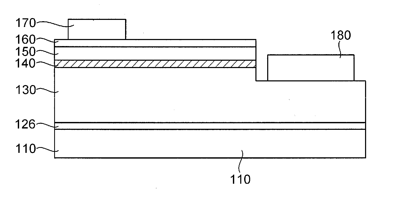
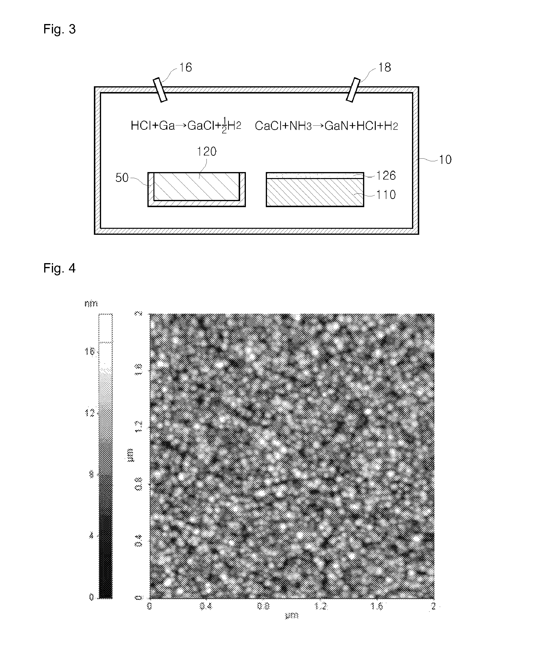
[0053]FIGS. 13 and 14 are schematic views illustrating a method for manufacturing a GaN based compliant substrate according to a second embodiment of the present invention. Particularly, the second embodiment exemplifies a process wherein a GaN layer is formed on the GaN based compliant substrate at a high temperature to illustrate an applicability of the compliant substrate.

[0054]Referring to FIG. 13, the compliant substrate having a GaN thin film 126 formed on a sapphire wafer 110 via a HVPE process is placed in a MOCVD reactor 20. A H2 gas and an NH3 gas are supplied through first and second inlets 24 and 26, respectively. A temperature of the MOCVD reactor 20 is elevated to 1050° C. and the temperature s maintained for approximately five minutes. Preferably, flow rates of the H2 gas and the NH3 gas are 30 liter / min and 6 liter / min, respectively. The temperature is elevated and maintained by a third heater.

[0055]Referring to FIG. 14, while supplying of the H2 gas and the NH3 gas ...


PUM

PropertyMeasurementUnit
thicknessaaaaaaaaaa
temperatureaaaaaaaaaa
thicknessaaaaaaaaaa

Abstract

A gallium nitride based compound semiconductor device including a compliant substrate having a reduced stress and a method for manufacturing the same are disclosed. The compliant substrate included in the gallium nitride based compound semiconductor device is manufactured by heating a substrate and a group III metal including at least one of an aluminum, a gallium and an indium, and a chloride based compound generated by introducing a HCl gas to the melted group III metal reacts with a NH3 gas to form a nitride based thin film on the wafer.

Description

TECHNICAL FIELD[0001]The present invention relates to a compliant substrate, a gallium nitride based compound semiconductor device including a compliant substrate and a method for manufacturing the same. More particularly, the present invention relates to a gallium nitride based compound semiconductor device including a compliant substrate and a method for manufacturing the same having a reduced manufacturing time and an improved work efficiency.BACKGROUND ART[0002]Generally, an AlGaInN, which is a gallium nitride based compound semiconductor including a small amount of an indium added thereto, is widely used for an active layer of a blue laser diode or a blue LED (light emitting diode).[0003]A 2-step MOVPE (metal organic vapor phase epitaxy) is a general method for controlling a growth of an AlGaInN crystal. In accordance with the method, the AlGaInN crystal is grown to a thickness of tens of nanometer (nm) on a sapphire substrate at a low temperature ranging approximately from 400...

Claims


Application Information

Patent Timeline
Patent Type & Authority Patents(United States)
IPC IPC(8): H01L21/20H01L21/36H01L31/0256H01L33/00
CPCC30B25/02C30B29/403H01L21/0237H01L21/0254H01L21/0262H01L21/02631H01L33/007
Inventor JIN, YONG SUNGLEE, JAE HAK
Owner THELEDS
Why Eureka
Try Eureka