Inductance analysis system and method and program therefor

a technology of inductance analysis and system, applied in the field of semiconductor device technology, can solve the problems of inductance analysis, limited application, and need of much time for analysis, and achieve the effect of short time and high accuracy on a large scal

Inactive Publication Date: 2010-10-26
LONGITUDE SEMICON S A R L
View PDF10 Cites 17 Cited by
  • Summary
  • Abstract
  • Description
  • Claims
  • Application Information

AI Technical Summary

Benefits of technology

[0012]In light of the above, it is envisaged by the present invention to provide a system, a method and a program for inductance analysis according to which it is possible to achieve shorter analysis time, to cope with an increased system size and to enable the analysis with high accuracy.
[0020]According to a seventh aspect of the present invention, there is provided a method for designing a multi-layered board including a power supply plane. The method includes a step of: placing a beginning point of non-coupled current of return current, associated with signal current, in the vicinity of the signal through-hole on the power supply plane, based on the position information of the signal through-hole. The method according to the present invention also includes a step of receiving information of the power supply plane and determining the potential distribution in the power supply plane, a step of receiving the information on the power supply plane and determining the potential distribution in the power supply plane, and a step of outputting the potential distribution in the power supply plane, thus determined. With the method according to the present invention, it is possible to evaluate the non-coupled inductance in the power supply plane from the signal through-hole to one or both of the power supply through-hole and the power supply via.
[0026]According to the present invention, in which the non-coupled inductance in a power supply plane is replaced by a resistance and potential analysis is carried out in the power supply plane to allow for evaluation and visualization of the non-coupled inductance. According to the present invention, analysis may be made highly accurately at a large scale and in a short time as compared to the case of inductance analysis by the analysis of the electromagnetic field.

Problems solved by technology

The conventional technique for inductance analysis, employing e.g. analysis of an electro-magnetic field, is in need of much time for analysis, and is limited to application with a small size of analysis.
Such state of the art poses a serious problem as regards the tool for analysis of the electro-magnetic field.

Method used


Image

  • Inductance analysis system and method and program therefor
  • Inductance analysis system and method and program therefor
  • Inductance analysis system and method and program therefor

Examples


Embodiment Construction

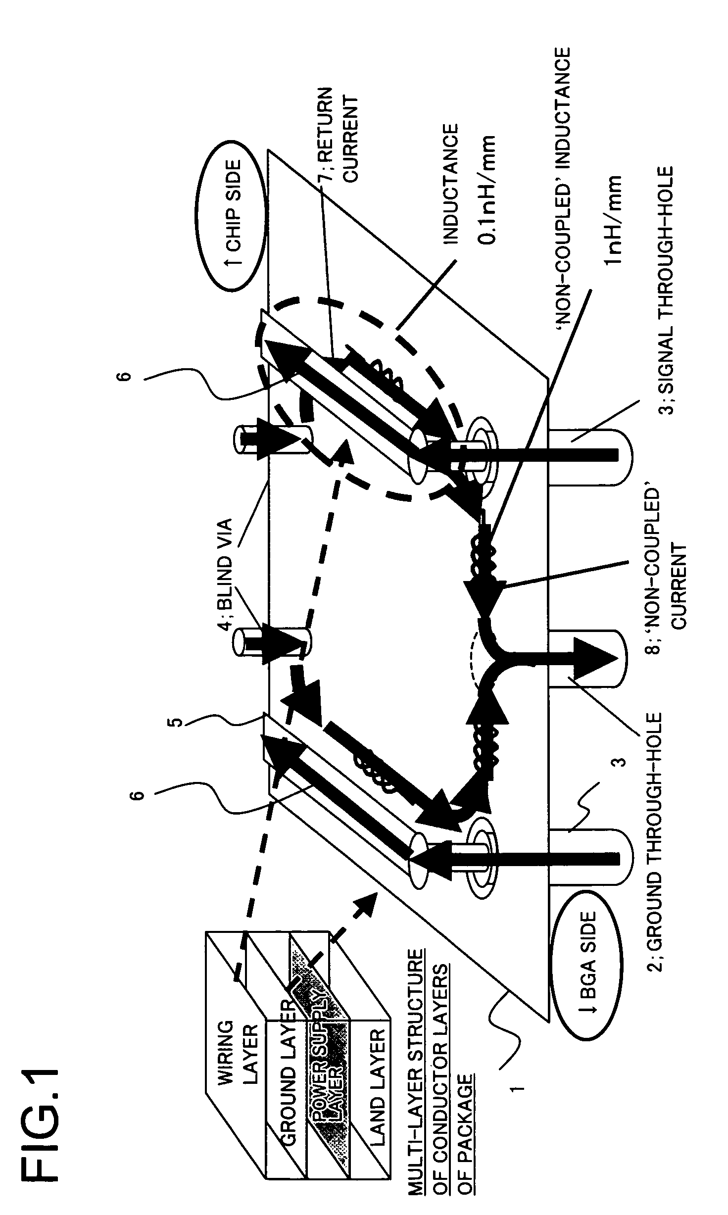
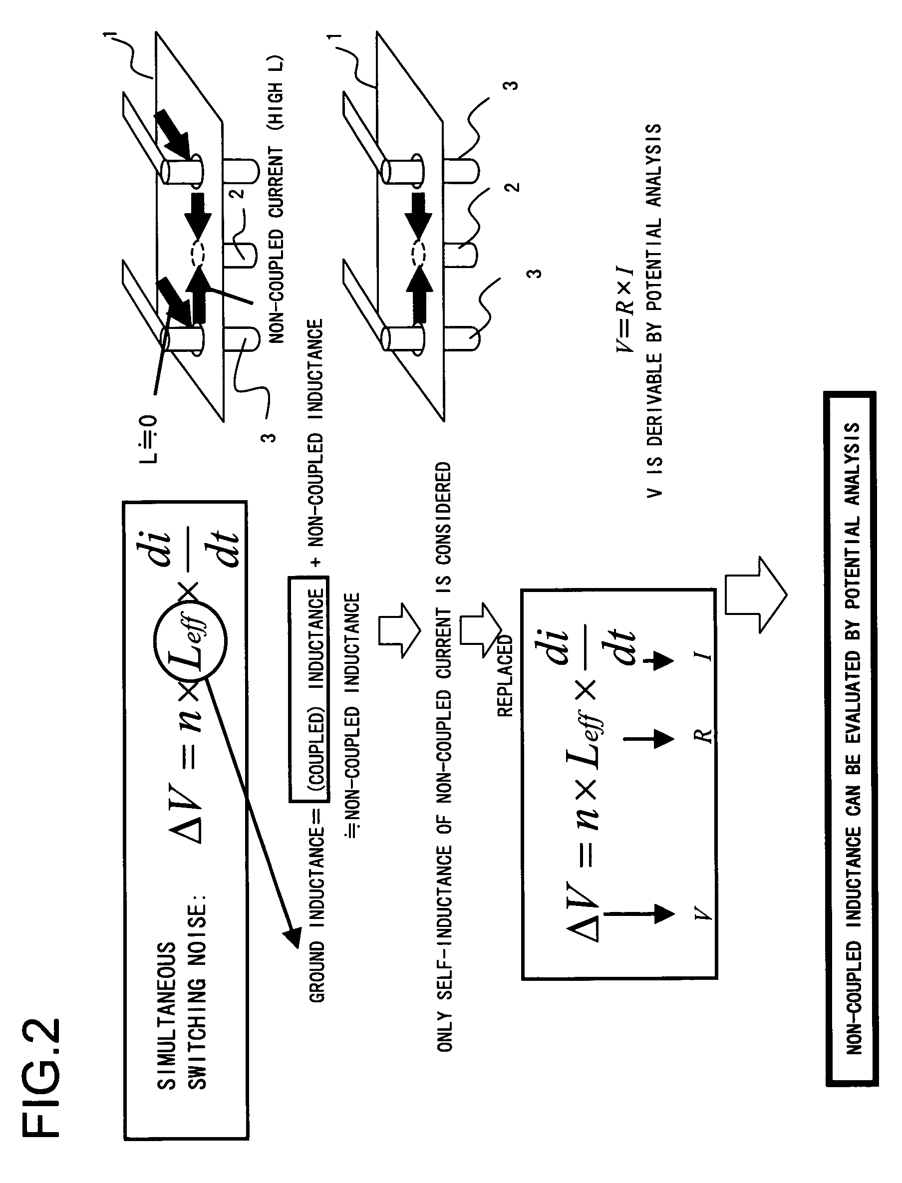
[0034]The present invention will now be described in detail with reference to the drawings. Referring to FIG. 1, signal through-holes 3 are passed through a ground plane 1. To this ground plane 1 are connected a ground through-hole 2 and blind vias 4. When signal current 6 flows through a signal wire 5 in a wiring layer, return current 7 flows on the ground plane 1 in a direction opposite to the direction along which flows the signal current 6. Due to a coupling electromagnetic field, the return current 7 flows through an area lying directly below the signal wire 6. However, the return current is not coupled to an electromagnetic field of non-coupled current 8 proceeding towards the ground through-hole 2, and hence the inductance (non-coupled inductance) is increased. That is, if there flows much non-coupled current, the ground inductance is increased. There are occasions where, for example, the non-coupled inductance is as high as 1 nH / mm for the coupled inductance of 0.1 nH / mm. Th...


PUM


Abstract

System, method and program for inductance analysis for reducing time for analysis, to cope with increase in the system size, to achieve high accuracy in the analysis. Information on a power supply plane, in a state in which a beginning point of non-coupled current of return current accompanying a signal current is placed in the vicinity of a signal through-hole on the power supply plane, based on position information of said signal through-hole, is received. Potential distribution in the power supply plane is determined and output. The non-coupled inductance from the signal through-hole to the power supply through-hole in the power supply plane is evaluated. In the potential analysis, non-coupled inductance L from the signal through-hole to the power supply through-hole is represented by resistance R. The relationship that a voltage increment ΔV is represented by the product of the non-coupled inductance L and the rate of time change of the current, ΔV=LΔI / Δt, is replaced by the relationship that the voltage V is represented by the product of resistance R and non-coupled current I, V=R×I. Potential analysis is performed by analyzing two-dimensional heat diffusion in the power supply plane assuming that a heat source is placed at a beginning point of the non-coupled current.

Description

FIELD OF THE INVENTION[0001]This invention relates to a technology for designing and manufacture of semiconductor devices. More particularly, this invention relates to a system, a method and a program for analysis convenient for e.g. a semiconductor package board.BACKGROUND OF THE INVENTION[0002]A package board, including a core layer and built-up layers and carrying a semiconductor chip and a BGA (ball grid array) terminal on its one major surface and on its opposite major surface, respectively, with an electrode of the semiconductor chip being extended to the BGA surface, has been in extensive use, because the power supply and the ground are provided as planes or layers, with the inductance and the noise being small. However, with increase in the operating frequency of the LSIs in these days, the power supply noise and the ground noise have increased. In particular, the simultaneous switching noise has become of a serious problem.[0003]Reference will now be made to FIG. 6. When a ...

Claims


Application Information

Patent Timeline
Patent Type & Authority Patents(United States)
IPC IPC(8): G06F17/50H01L23/52
CPCG06F17/5036H05K1/115H05K3/0005G06F30/367
Inventor KATAGIRI, MITSUAKIIIDA, TAKASHISHIMIZU, HIROYAISA, SATOSHI
Owner LONGITUDE SEMICON S A R L
Why Eureka
Try Eureka