Bipolar complementary semiconductor device

a complementary semiconductor and bipolar technology, applied in the direction of semiconductors, semiconductor devices, electrical devices, etc., can solve the problems of reducing the operation efficiency of pnp, reducing the efficiency of cmos, etc., to achieve the effect of reducing resistance, high frequency properties and simple production

Active Publication Date: 2010-12-21
IHP GMBH INNOVATIONS FOR HIGH PERFORMANCE MICROELECTRONICS LEIBNIZ INST FUR INNOVATIVE
View PDF12 Cites 10 Cited by
  • Summary
  • Abstract
  • Description
  • Claims
  • Application Information

AI Technical Summary

Benefits of technology

[0065]Particularly preferably one or more of the layers of the base layer stack is or are doped with carbon. The dopant concentration in the carbon-doped layers can be increased in that way, which provides for a reduction in the resistance and is beneficial to the high frequency properties of both bipolar transistor types.
[0066]The first, the second or both transistor types can include a T-shaped emitter. An...

Problems solved by technology

a) Good high frequency properties in the case of npn-transistors fit in with the type of the heterojunction of Si/SiGe, while that kind of heterojunction can adversely affect the operational efficiency of pnp-transistors, see D V Singh, J L Hoyt and J F Gibbons: ‘Novel epitaxial p-Si/n-Si1-yCy/p-Si heterojunction bipolar transistors’, IEDM 2000, pages 749-752 or D V Singh, J L Hoyt and J F Gibbons: ‘Effect of band alignment and density of states on the collector current in p-Si/n-Si1-yCy/p-SiHBTs’, IEEE Trans. Electron. Devices, Vol 50, pages 425-432, February 2003.
b) By virtue of the deposit and diffusion properties of the respective dopants, the demands on the doping profile of npn-high-speed transistors can be more easily satisfied in a BiCMOS process, than those for a pnp-transistor.
c) The process complexity of conventional complementary bipolar or BiCMOS processes is so great and the mutual influence of the process modules on device parameters is so considerable that there are few approaches which aim at an improvement in the high frequency properties of pnp-transistors in a CBIMOS semiconductor device.
A disadvantage of that process however is that typical modern CMOS technologies do not include either epitaxially buried collector layers or deep insulation trenches or collector sinkers.
The process expenditure for those process steps is in part considerable.
As the CMOS transistors are introduced into the epitaxy layer which is deposited over the buried collector layers, an additional heat loading of the buried collector layers used by El-Kareh et al during the CMOS process cannot be avoided.
That reduces the profile gradient of the buried collector layers, whereby the efficiency of both bipolar transistor types but in particular that of the pnp-transistors in the high-speed range is adversely affected.
Furthermore the process described by El-Kareh et al suffers from the disadvantage that proc...

Method used


Image

  • Bipolar complementary semiconductor device
  • Bipolar complementary semiconductor device
  • Bipolar complementary semiconductor device

Examples


example 1

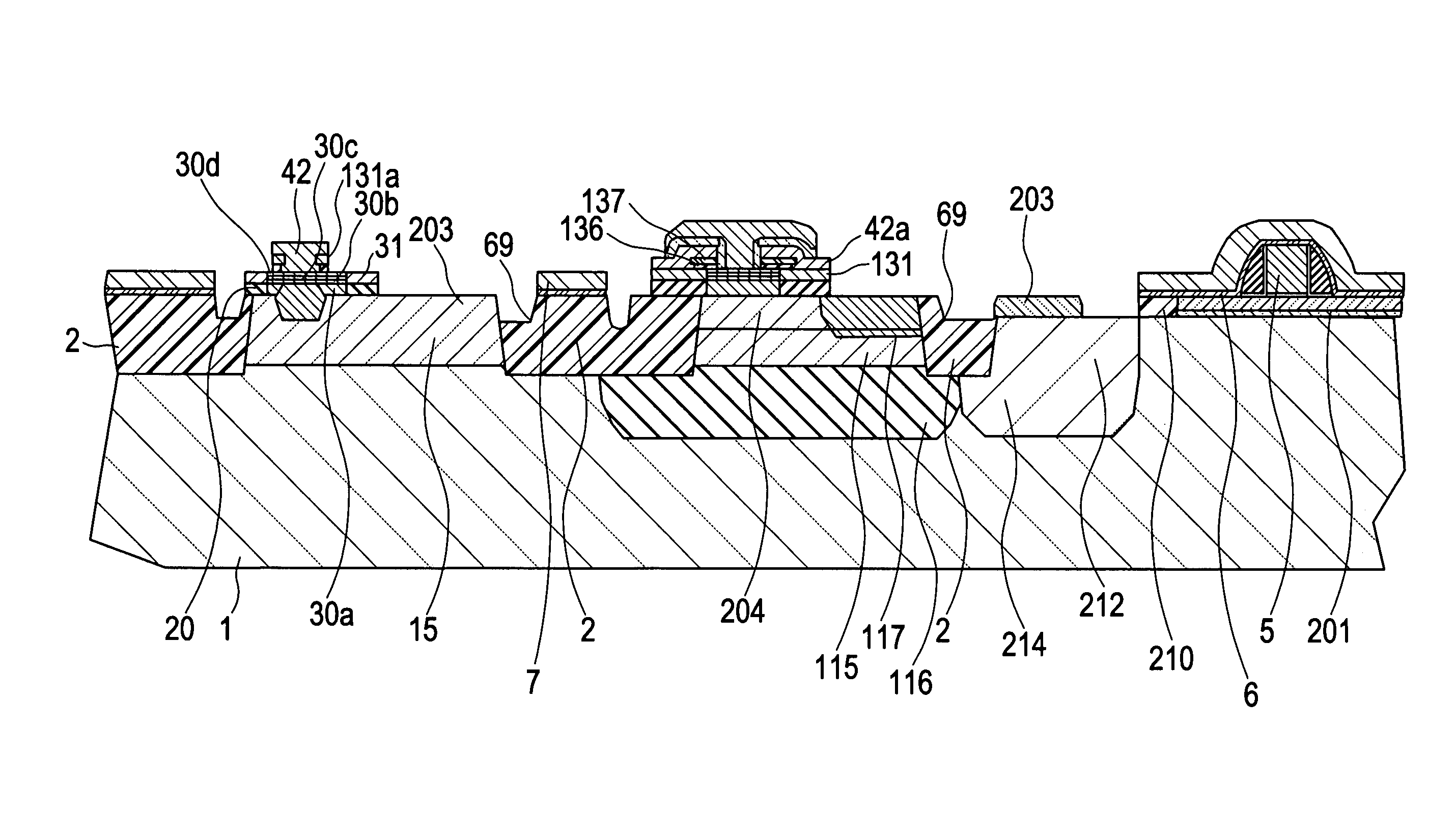
[0100]An embodiment of the semiconductor device according to the invention which includes complementary bipolar transistors with an epitaxial base is now described with reference to FIG. 1. In this example an npn-bipolar transistor A and a pnp-bipolar transistor B are produced on a high-ohmic monocrystalline p−-conductive Si substrate 1. The arrangement described here is not restricted to p−-conductive Si substrates. The essential features can also be transferred to substrates of the opposite conductivity type. At the same time CMOS transistors can also be present on the substrate 1, but are not shown in FIG. 1.

[0101]The npn-bipolar transistor A with an epitaxial base includes an n-conducting collector 11 and an also n-conducting emitter 40. The collector is passed for contact laterally by way of the collector contact region 12 and a collector connection doping 14.

[0102]In the vertical direction between the emitter 4 and the collector 11 is a monocrystalline layer stack 30 which is ...

example 2

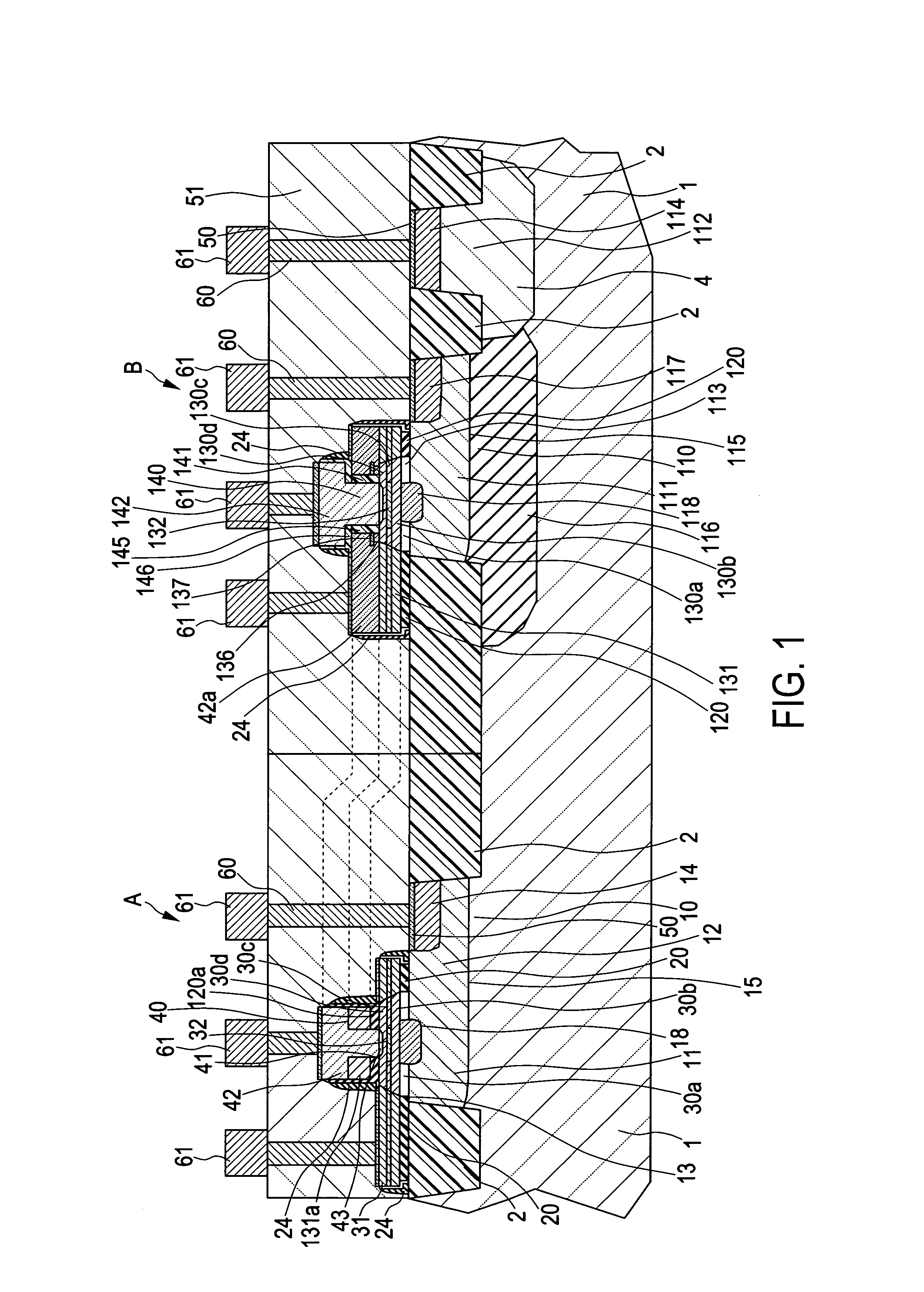
[0127]Reference will now be made to FIGS. 2 through 8 to describe a process for the production of the semiconductor device according to the invention comprising complementary bipolar transistors with an epitaxial base. In addition in the example set forth here MOS transistors are also produced on one and the same substrate wafer besides complementary bipolar transistors.

[0128]FIG. 2 shows a snapshot during a first masking step for the production of complementary bipolar transistors. The basis for production is formed by a substrate 1 (FIG. 2) which preferably includes a monocrystalline p−-conducting (low p-conducting doping) silicon which is as high-ohmic as possible. The processing procedure for the substrate 1 begins with the production of the field insulation regions 2. In the present embodiment so-called shallow trenches are used as the field insulation regions. Selected regions have been doped by implantation in the further course of the production process. On those regions, re...

example 3

[0159]The procedure set forth in Example 2 is modified in such a way that, prior to the deposit of the layer stack 6, 7, no gate spacers are produced at the MOS gates. Production of gate spacers can be effected on the one hand with the removal of the layer 7 at the end of the bipolar module. In that respect it is not a wet etching process but a dry etching step that is required, unlike Example 2. On the other hand, as described in Example 2, a layer can be deposited after the bipolar module, which is used by means of a dry etching step for the gate spacer production operation. As set forth in Example 2 defined regions can be protected prior to that etching operation if a lacquer mask is structured beforehand.


PUM


Abstract

A complementary BiCMOS semiconductor device comprises a substrate of a first conductivity type and a number of active regions which are provided therein and which are delimited in the lateral direction by shallow field insulation regions, in which vertical npn-bipolar transistors with an epitaxial base are arranged in a first subnumber of the active regions and vertical pnp-bipolar transistors with an epitaxial base are arranged in a second subnumber of the active regions, wherein either one transistor type or both transistor types have both a collector region and also a collector contact region in one and the same respective active region. To improve the high-frequency properties exclusively in a first transistor type in which the conductivity type of the substrate is identical to that of the collector region, an insulation doping region is provided between the collector region and the substrate.

Description

CROSS REFERENCE TO RELATED APPLICATIONS[0001]This application is for entry into the U.S. national phase under §371 for International Application No. PCT / EP2004 / 013855 having an international filing date of Dec. 1, 2004, and from which priority is claimed under all applicable sections of Title 35 of the United States Code including, but not limited to, Sections 120, 363 and 365(c), and which in turn claims priority under 35 USC §119 to German Patent Application No. 103 58 047.6 filed on Dec. 5, 2003.BACKGROUND OF THE INVENTION[0002]1. Technical Field[0003]The invention concerns a complementary bipolar semiconductor device, hereinafter also referred to as a CBi semiconductor device, comprising a substrate of a first conductivity type and a number of active regions which are provided therein and which are delimited in the lateral direction by shallow field insulation regions, in which vertical npn-bipolar transistors with an epitaxial base are arranged in a first subnumber of the activ...

Claims


Application Information

Patent Timeline
IPC IPC(8): H01L29/80H01L31/112H01L21/8228H01L21/8249H01L27/06H01L27/082
CPCH01L21/82285H01L21/8249H01L27/0623H01L27/0826
Inventor HEINENMAN, BERNDDREWS, JÜRGENMARSCHMAYER, STEFFENRÜCKER, HOLGER
Owner IHP GMBH INNOVATIONS FOR HIGH PERFORMANCE MICROELECTRONICS LEIBNIZ INST FUR INNOVATIVE
Why Eureka
Try Eureka