Hybrid broadband power amplifier with capacitor matching network

Active Publication Date: 2011-03-22
CW ACQUISITION
View PDF3 Cites 33 Cited by
  • Summary
  • Abstract
  • Description
  • Claims
  • Application Information

AI Technical Summary

Benefits of technology

[0006]Multi-section transmission line matching networks are typically used for broadband power amplifiers. The section closest to the power transistor normally has the lowest impedance. The line is typically very wide to achieve the low impedance on the common ceramic substrat

Problems solved by technology

However, GaN transistors are very small due to its high power density.
The dimensional mismatch between the low impedance transm

Method used


Image

  • Hybrid broadband power amplifier with capacitor matching network
  • Hybrid broadband power amplifier with capacitor matching network
  • Hybrid broadband power amplifier with capacitor matching network

Examples


Example

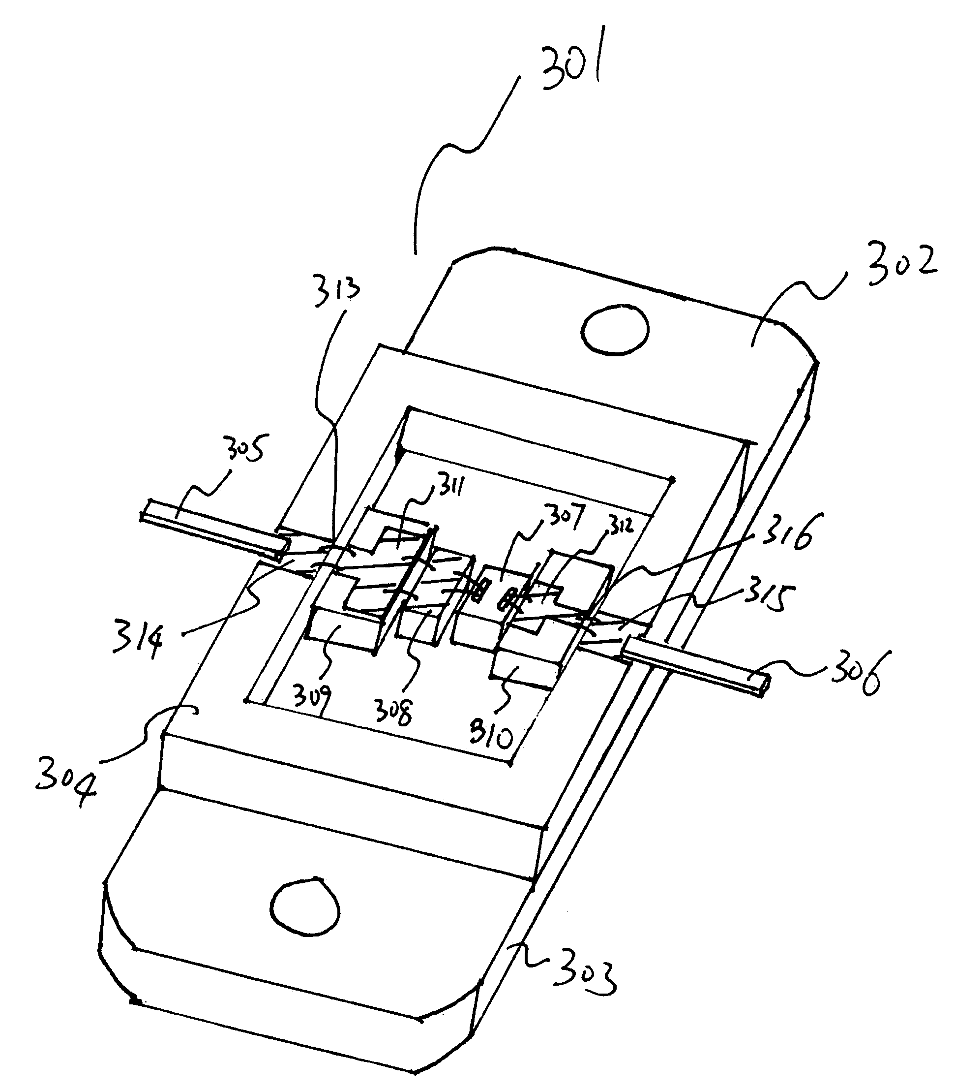
[0014]The traditional high power transistors typically have very low optimum source and load impedance for maximum output power. GaN transistors have very high breakdown voltage and hence have higher optimum source / load impedance comparing to the sub-Ohm impedance from conventional transistors such as GaAs FET or Silicon LDMOS. However, the optimum source and load impedance is still low for high power GaN devices. Especially the real part of the optimum source impedance being in the range of only a few Ohms for a GaN device with more than 10 Watts of output power capability.

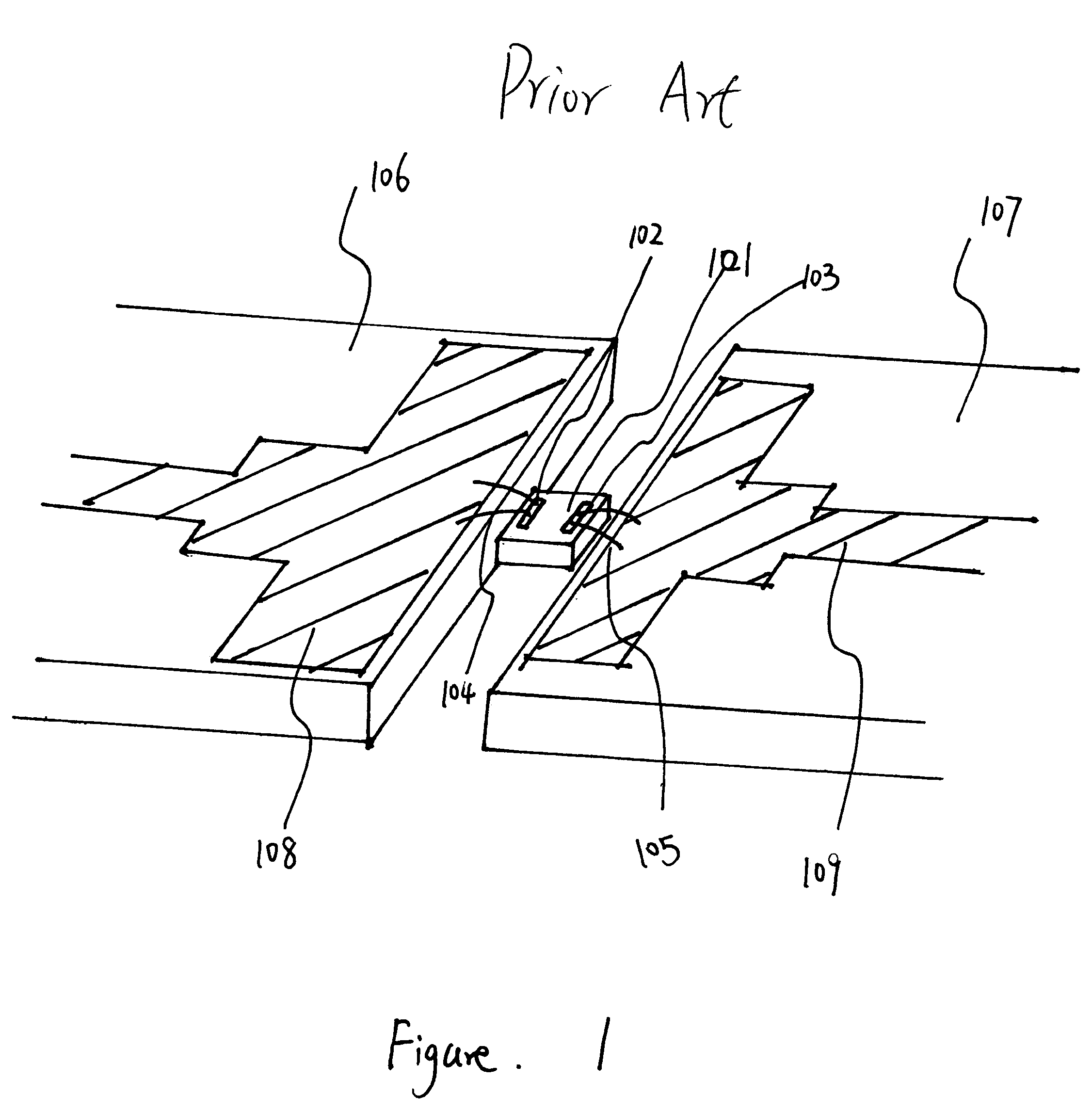
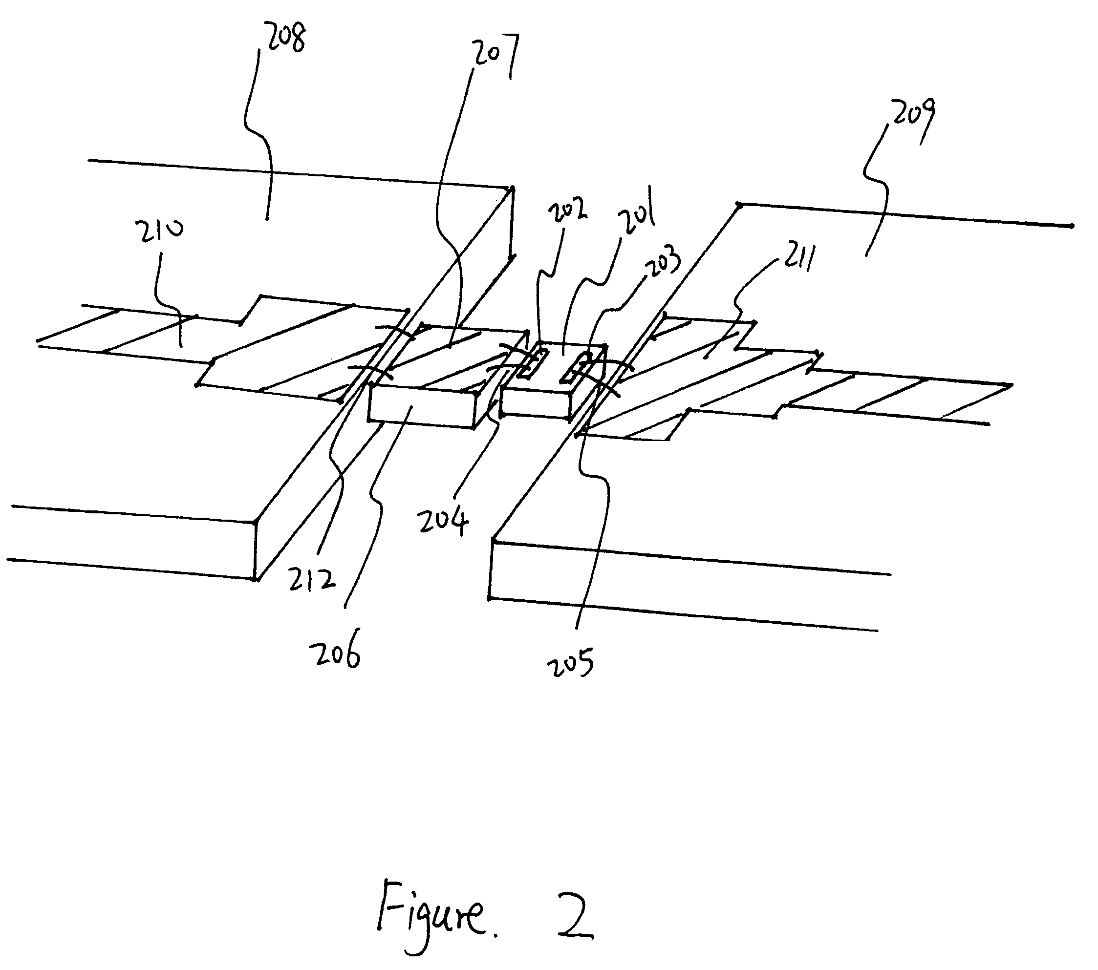
[0015]Multi-section transmission line matching networks are typically used for broadband power amplifiers. The matching network has several sections. Each section is around quarter lambda in length (lambda is the wavelength on the substrate at the center frequency). The matching network transforms the port impedance (typically 50 Ohm) to the optimum source and load impedance. The section closest to the power tran...


PUM


Abstract

A hybrid broadband power amplifier module design is disclosed. In a power amplifier design, low impedance transmission lines are typically needed at the input and output of the transistor to match for its optimum source and load impedance. The peripheral of the GaN (Gallium Nitride) transistor is very small due to the high power density of the GaN transistor. The transmission line, for example a microstrip line, needs to be very wide to achieve low impedance on ceramic substrates such as Alumina. The dimensional mismatch from the low impedance transmission line to the transistor causes additional parasitic effect to the matching networks and limits the bandwidth of the amplifier. Capacitor materials are typically very high in dielectric constant; hence a single layer capacitor with small dimensions equalizes to a low impedance transmission line. Selected capacitors with proper dimensions can be used as the low impedance transmission lines in the matching networks. They will have comparable width to the GaN transistor and minimize the parasitic effect. The wavelength inside the capacitor will also be very short due to the high dielectric constant; hence the matching network can be much shorter. A compact hybrid amplifier module has been built in a small package with the GaN transistor, capacitor matching networks and other necessary circuits inside. More than an octave bandwidth can be achieved with this new scheme.

Description

[0001]This application claim an invention disclosed in prior-filed provisional application (Application No. 61 / 013,997) filed Dec. 14, 2007.BACKGROUND OF THE INVENTION[0002]1. Field of Invention[0003]This invention relates to a power amplifier module design using transistor, capacitor, matching network and package.[0004]2. Description of Prior Art[0005]A hybrid power amplifier typically includes a transistor, an input matching network and an output matching network. The input / output matching networks transform the input / output port impedance (typically 50 Ohm) to the optimum source / load impedance of the transistor to achieve the maximum output power. The matching networks typically need to have a characteristic impedance of a few Ohms to transform the port impedance to the optimum load impedance of a high power device. The input / output matching networks are typically printed on ceramic substrate such as Alumina (Al2O3). The bandwidth of the power amplifier is normally less than an o...

Claims


Application Information

Patent Timeline
IPC IPC(8): H03F1/00
CPCH01L23/66H01L24/49H03H7/38H03F3/60H03F3/195H03F1/56H01L2924/30107H01L2924/13064H01L2924/01006H01L24/48H03F2200/387H03F2200/36H03F2200/222H01L2223/6627H01L2223/6644H01L2223/6655H01L2224/48091H01L2224/48227H01L2224/4911H01L2224/49171H01L2924/01014H01L2924/01031H01L2924/01078H01L2924/10329H01L2924/1033H01L2924/1903H01L2924/19032H01L2924/19041H01L2924/19107H01L2924/3011H01L2924/00014H01L2924/00H01L2924/15787H01L2924/30111H01L2224/05599H01L2224/85399H01L2224/45015H01L2924/207H01L2224/45099
Inventor JIA, PENGCHENG
Owner CW ACQUISITION
Why Eureka
Try Eureka