Anisotropic conductive film, method for producing the same, and bonded structure

a technology of anisotropic conductive film and conductive particle, applied in the direction of conductors, light beam reproducing, instruments, etc., can solve the problems of high conduction reliability, conductive particle movement along, short circuit, etc., to prevent short circuit, high particle capture ratio, and excellent conduction reliability

Active Publication Date: 2011-04-26
SONY 50
View PDF7 Cites 5 Cited by
  • Summary
  • Abstract
  • Description
  • Claims
  • Application Information

AI Technical Summary

Benefits of technology

[0014]The present invention aims at solving the problems arisen in the conventional art, and achieving the following object. Namely, the object of the present invention is to provide a two-layered anisotropic conductive film which prevents the movement of conductive particles when used for bonding an electronic part and a substrate, etc., so as to prevent a short circuit, assures a high particle capturing ratio so as to attain excellent conduction reliability, and is easily handled. Another object of the present invention is to provide an efficient production method of the anisotropic conductive film, and a bonded structure of an electronic part and a substrate, etc., using the anisotropic conductive film, which has a high particle capturing ratio and excellent conduction reliability.
[0018]Therefore, the conductive particles are fixed in a portion adjacent to the interface with the insulating layer in the state where the conductive particles are aligned into a monolayer. When the anisotropic conductive film of the present invention is used for connecting an electronic part and a substrate, etc., the conductive particles are not moved when pressed and bonded, the conductive particles are captured by terminals at a high particle capturing ratio, and thus excellent conduction reliability is assured and it can be sufficiently applicable to terminals of narrower pitch. Moreover, as the side of the conductive particle-contained layer where the conductive p articles are not present is in the state of the low degree of cure and / or in the uncured state, the photo and thermal curing resin composition has adhesiveness, and can easily bonded to the substrate or the like, the anisotropic conductive film of the present invention is very conveniently used as it has the same functions as to the conventional three-layered anisotropic conductive film even though it is of two-layered structure.
[0025]According to the method for producing in anisotropic conductive film of <7>, conductive particles are aligned into a monolayer at one side of a layer containing a photo and thermal curing resin composition, and the one side of the layer is exposed to curing light so as to form a conductive particle-contained layer, and an insulating layer formed of an insulating resin composition is laminated on the one side of the conductive particle-contained layer. As a result, an anisotropic conductive film is efficiently produced.
[0031]In the bonded structure of <12>, at least two selected from the electronic parts and the substrates are electrically connected by using the anisotropic conductive film of the present invention, a particle capturing ratio of the conductive particle is high and thus conduction reliability is excellent.
[0034]According to the present invention, the problems in the art can be solved, and a two-layered conductive film which prevents the movement of conductive particles when used for bonding an electronic part and a substrate, etc., so as to prevent a short circuit, assures a high particle capturing ratio so as to attain excellent conduction reliability, and is easily handled can be provided. According to the present invention there are also provided an efficient production method of the anisotropic conductive film, and a bonded structure of an electronic part and a substrate, etc., using the anisotropic conductive film, which has a high particle capturing ratio and excellent conduction reliability.

Problems solved by technology

Even though the connection area is reduced, reliability for high conduction is still required.
However, the single-layered anisotropic conductive adhesion film has a problem such that conductive particles are moved along with the insulation adhesive by the heat and pressure at the time of the connection.
However, pitch between terminals of electronic devices has been getting smaller and smaller as a trend, and if the two-layered anisotropic conductive adhesion film is used in such the electronic device, conductive particles are moved along with an insulating adhesive to the surrounding of IC chip by heat pressure at the time of the connection and the moved into the gap between terminals, causing a short circuit.
Moreover, it is also insufficient in terms of the particle capturing rate.
Moreover, it is difficult to accurately form the conductive particle layer at the thickness of 5 μm or less using a normal roll coater or comma coater.
The insulating adhesive layer disclosed in JP-A No. 2003-64324 is cured by the radiation of actinic light, but is not cured and has adhesiveness before use.

Method used


Image

  • Anisotropic conductive film, method for producing the same, and bonded structure
  • Anisotropic conductive film, method for producing the same, and bonded structure
  • Anisotropic conductive film, method for producing the same, and bonded structure

Examples


example 1

-Production of Anisotropic Conductive Film-

[0151]A coating solution of a conductive particle-contained layer was prepared using the ingredients shown in Table 1 below.

[0152]

TABLE 1ProportionIngredients(part(s) by mass)Acryl polymer(1604N, manufactured by70Soken Chemical & Engineering Co., Ltd.)Acryl monomer(3002A, manufactured by30Kyoeisha Chemical Co., Ltd.)Photopolymerization initiator(IRGANOX ®1369, manufactured by Chiba Japan K.K.)Thermoset initiator(PERHEXA 3M,4manufactured by NOF Corporation)Toluene100Total205

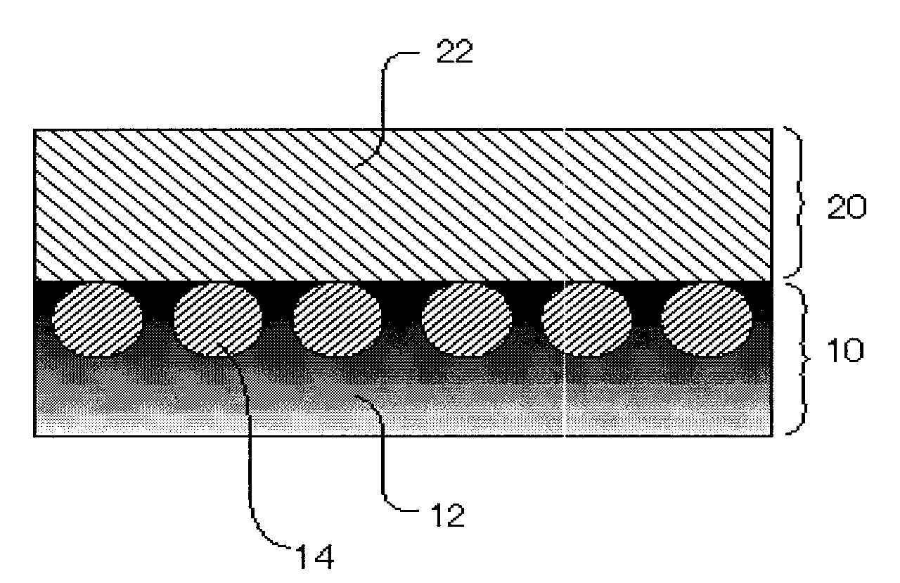
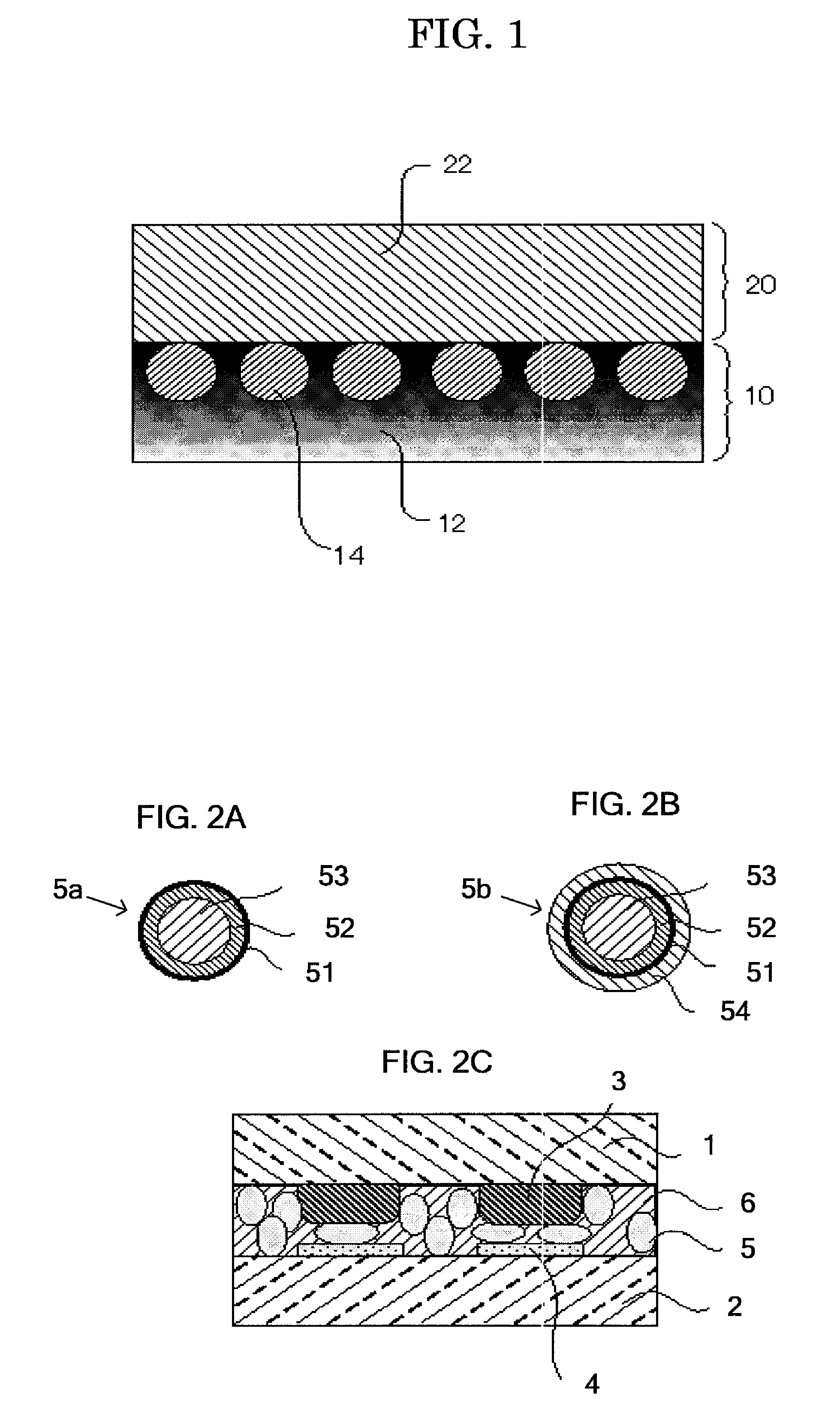
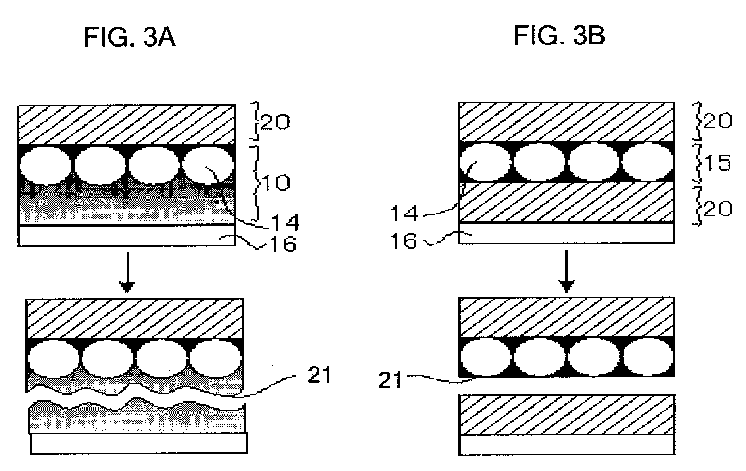
[0153]The thus obtained coating solution of a conductive particle-contained layer was applied onto a releasable PET sheet S1 using a bar coater, and dried at 60° C. for 10 minutes so as to evaporate the solvent contained therein, to thereby obtain a film A having a thickness of 10 μm (seeFIG. 5A). The surface of the thus obtained film A had tackiness.

[0154]Subsequentially, 50 g of Ni—Au plating conductive particles P (BRIGHT GNR-EHLCD, manufactured by Nippon Chemical Indu...

example 2

-Production of Anisotropic Conductive Film-

[0163]An anisotropic conductive film was produced in the same manner as in Example 1, provided that the conductive particle-contained layer forming step was performed in the following manner.

[0164]A coating solution of a conductive particle-contained layer was prepared based upon the ingredients shown in Table 3.

[0165]

TABLE 3ProportionIngredients(part(s) by mass)Bifunctional acryl monomer (CN112C60,70manufactured by Sartomer Company, Inc.)Phenoxy resin (PKHH, manufactured by30Union Carbide Corporation)Photopolymerization initiator (IRGACURE ®1369, manufactured by Chiba Japan K.K.)Thermoset initiator(organic peroxide)4(PERHEXA 3M, manufactured by NOF Corporation)Conductive particle(BRIGHT GNR-EHLCD,80diameter of 4 μm, manufactured by NipponChemical Industrial Co., Ltd.)Toluene100Total285

[0166]The thus obtained coating solution of a conductive particle-contained layer was applied onto a releasable PET sheet S6 using a bar coater, and dried in...

example 3

[0169]An anisotropic conductive film was produced in the same manner as in Example 1, provided that the ingredients of a coating solution for the conductive particle-contained layer used in Example 1 was replaced with the ingredients shown in Table 4, and a carbon black was added to the ingredients as the curing light absorbent.

[0170]A coating solution for a conductive particle-contained layer was prepared based upon the ingredients shown in Table 4.

[0171]

TABLE 4ProportionIngredients(part(s) by mass)Acryl polymer (PML103, manufactured by Soken55Chemical & Engineering Co., Ltd.)Acryl monomer45(M450, manufactured by Toagosei Co., Ltd.)Photopolymerization initiator (IRGANOX ®1369, manufactured by Chiba Japan K.K.)Thermoset initiator4(PERHEXA 3M, manufactured by NOF Corporation)Curing light absorbent (carbon black)1(Asahi-Thermal, manufactured by Asahi CarbonCo., Ltd., average particle size: 80 nm)Toluene100Total206

[0172]The thus obtained coating solution for EL conductive particle-cont...


PUM

PropertyMeasurementUnit
total thicknessaaaaaaaaaa
particle sizeaaaaaaaaaa

Abstract

Provided is an anisotropic conductive film, containing: an insulating layer formed of an insulating resin composition; and a conductive particle-contained layer containing a photo and thermal curing resin composition and conductive particles, the conductive particles being aligned into a monolayer in a portion adjacent to an interface with the insulating layer, in which the conductive particle-contained layer has a degree of cure which is gradually lowered in a thickness direction of the conductive particle-contained layer, from the side where the conductive particles are present to the side where the conductive particles are not present.

Description

CROSS-REFERENCE TO RELATED APPLICATION[0001]This is a continuation of Application No. PCT / JP2008 / 060738, filed on Jun. 12, 2008.BACKGROUND OF THE INVENTION[0002]1. Field of the Invention[0003]The present invention relates to an anisotropic conductive film that is capable of electrically and physically connecting between an electronic part of IC chip or a liquid crystal panel (LDC panel) of a liquid crystal display (LCD) and a substrate, or between substrates, and also relates to a method for efficiently producing the anisotropic conductive film, and a bonded structure for the electronic part and the substrate, etc. using the anisotropic conductive film.[0004]2. Description of the Related Art[0005]Anisotropic conductive adhesion films (ACF: Anisotropic Conductive Film) have conventionally been used as a means for connecting an electronic part and a circuit substrate. The anisotropic conductive adhesion film is used for adhering and electrically connecting between various terminals, f...

Claims


Application Information

Patent Timeline
Patent Type & Authority Patents(United States)
IPC IPC(8): B32B5/16B32B27/30B32B27/38B32B37/06
CPCH05K3/323Y10T428/26Y10T428/25Y10T428/265Y10T428/31511H01B5/16H01R11/01H01R43/00
Inventor FUJITA, YASUHIRO
Owner SONY 50
Why Eureka
Try Eureka