

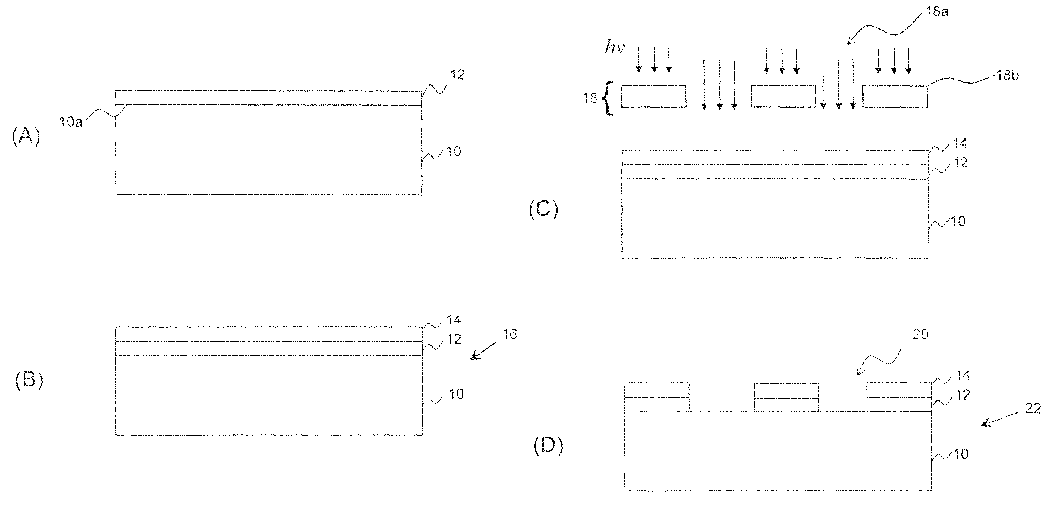
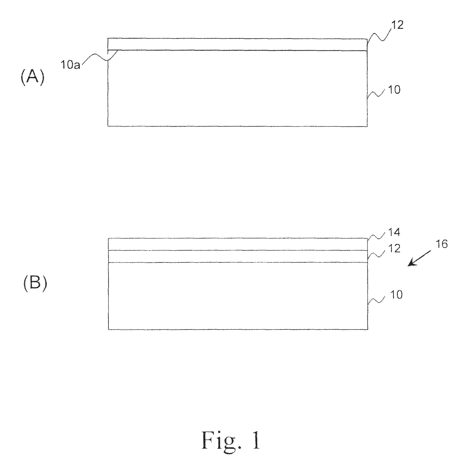
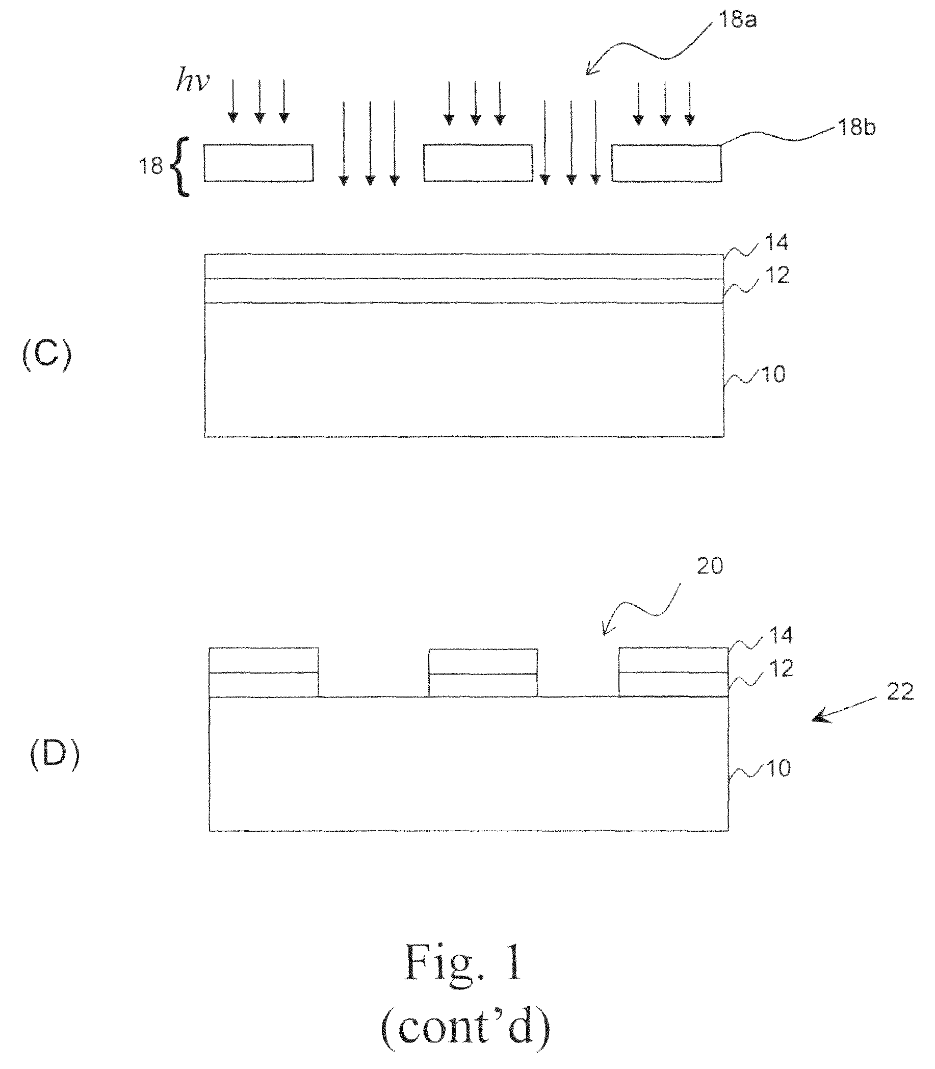
Photosensitive hardmask for microlithography
a microlithography and hardmask technology, applied in the field of photosens, can solve the problems of reducing the thickness of the photoresist, unable to offer sufficient etch resistance, and the current-available photoresist still etchs relatively quickly, so as to shorten the process time, less time, and less cost
- Summary
- Abstract
- Description
- Claims
- Application Information
AI Technical Summary
Benefits of technology
Problems solved by technology
Method used
Image

Examples
example 1
Hardmask Formulation I
[0053]In this procedure, a photosensitive hardmask was formulated by first diluting 3.5 grams of isopropanol solution of colloidal silica (˜30 wt % SiO2, average particle size 10-15 nm) (Organosilicasol™ IPA-ST; obtained from Nissan Chemical, Houston, Tex.) with 5 ml of PGME (obtained from Harcros Chemicals, St. Louis, Mo.). Then, 350 mg of trifunctional vinyl ether crosslinker (see Example 8) were added into the solution, together with 5 mg of pyridinium p-toluenesulfonate (PPTS; obtained from Aldrich, Milwaukee, Wis.). The mixture was stirred overnight at room temperature in a glass vial and then diluted further with PGME to a total solution weight of 56 grams. Next, 20 mg of triethanolamine (TEA; obtained from Aldrich, Milwaukee, Wis.) and 26 mg of the PAG di-(p-t-butylphenyl) iodonium tris(perfluoromethanesulfonyl)methide (DTBPI-C1; obtained from DAYCHEM Laboratories, Inc., Vandalia, Ohio) were added. This final formulation was filtered through a particle f...
example 2
Hardmask Formulation 2 and Photosensitivity Test
[0057]In this procedure, a second hardmask formulation was prepared by adding 10 mg of DTBPI-C1 PAG to 10 mg of hardmask Formulation 1 from Example 1 above to produce a more photosensitive Formulation 2. The formulation was spin-coated at 2,000 rpm onto a silicon substrate and then baked at 130° C. for 60 seconds. The film was then exposed to UV light through a 248-nm filter for various periods of time (i.e., 5, 8, 10, and 12 seconds). After PEB at 130° C. for 60 seconds and development using PD523AD, the remaining thickness (in nanometers) of the exposed areas was measured and plotted against the exposure dose (in mJ / cm2). The representative contrast curve shown in FIG. 2 clearly indicates the sharp contrast of developer solubility before and after the exposure dose reached 25 mJ / cm2.
example 3
Imaging Using Formulation 2 on Anti-reflective Coating Material
[0058]In this procedure, a structure was prepared and patterned using hardmask Formulation 2 from Example 2 above. First, an anti-reflective coating material (ARC® 29A; obtained from Brewer Science, Inc., Rolla, Mo.) was spin-coated onto a silicon wafer at 2,500 rpm, followed by baking at 205° C. The anti-reflective coating had a thickness of 80 nm. Formulation 2 was spin-coated at 2,000 rpm on top of the ARC® 29A coating and then baked at 130° C. for 60 seconds. The film stack was exposed to UV light through a 248-nm filter to give an exposure of >25 mJ / cm2 (according to the contrast curve in FIG. 2). After PEB at 130° C. for 60 seconds and development using PD523AD, the resulting patterns were imaged under optical microscopy to give FIG. 3, which shows positive micropatterns (down to 10-μm lines) that were resolved using hardmask Formulation 2.
PUM
| Property | Measurement | Unit |
|---|---|---|
| particle size | aaaaa | aaaaa |
| sizes | aaaaa | aaaaa |
| wavelengths | aaaaa | aaaaa |
Abstract
Description
Claims
Application Information