Manufacturing method for silicon wafer

a manufacturing method and silicon wafer technology, applied in the direction of polycrystalline material growth, crystal growth process, after-treatment details, etc., can solve the problems of poor productivity, increased requirements for silicon wafer quality to be used as a substrate of such semiconductor devices, and increased production costs, so as to reduce the growth defect, improve the surface roughness of silicon wafer, and suppress the generation of slip

Active Publication Date: 2011-07-12
GLOBALWAFERS JAPAN
View PDF9 Cites 2 Cited by
  • Summary
  • Abstract
  • Description
  • Claims
  • Application Information

AI Technical Summary

Benefits of technology

[0013]In view of the above situation, the invention has been made. An object of the invention is to provide a manufacturing method for a silicon wafer capable of reducing a grown-in defect while suppressing generation of slip during a rapid heating / cooling thermal process and in addition, capable of improving surface roughness of the silicon wafer obtained by the rapid heating / cooling thermal process.
[0039]The present invention provides a manufacturing method for a silicon wafer capable of reducing a grown-in defect while preventing generation of slip during a rapid heating / cooling thermal process and in addition improving surface roughness of the silicon wafer obtained by the rapid heating / cooling thermal process.

Problems solved by technology

With trends toward high integration of semiconductor devices in recent years, requirement for quality of a silicon wafer to be used as a substrate of such semiconductor devices is becoming severer.
The heat treatment technique described in the JP-A-11-260677 is however not preferred because it has poor productivity because long heat treatment time is necessary and in addition, slip tends to occur during heat treatment.
The heat treatment technique described in the JP-A-2001-144275 is also not preferred because it has also poor productivity due to a substantially long heat treatment time and in addition, slip tends to occur during heat treatment.

Method used


Image

  • Manufacturing method for silicon wafer
  • Manufacturing method for silicon wafer
  • Manufacturing method for silicon wafer

Examples


first embodiment

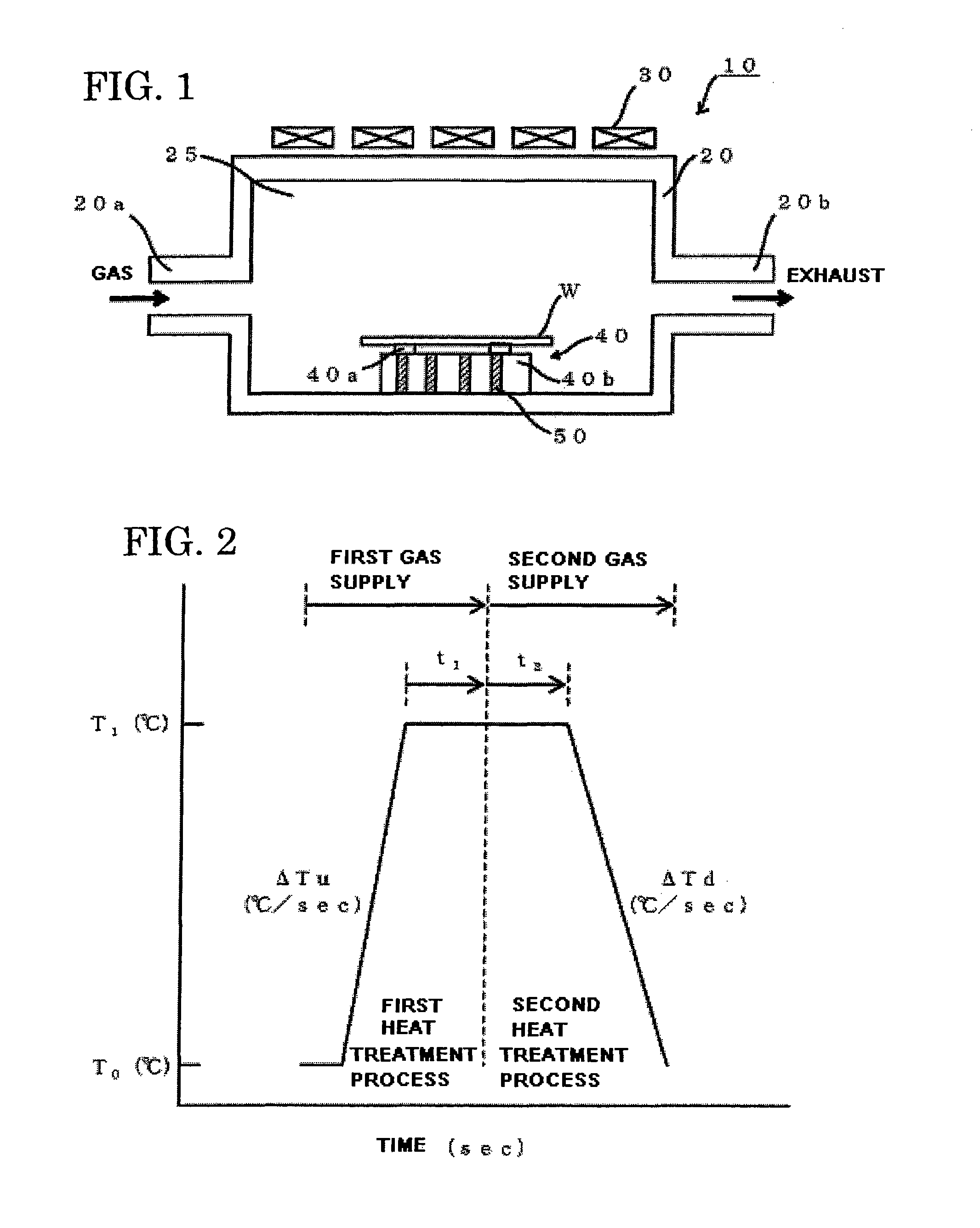
[0054]The manufacturing method for a silicon wafer according to a first embodiment of the invention will hereinafter be described referring to accompanying drawings.

[0055]The manufacturing method for a silicon wafer according to the first embodiment of the invention includes subjecting a silicon wafer produced from a silicon single crystal ingot grown by the Czochralski process to a rapid heating / cooling thermal process under particular production conditions.

[0056]Growing of the silicon single crystal ingot by the Czochralski process is performed in a known manner.

[0057]Described specifically, the silicon single crystal ingot is produced by heating polycrystalline silicon filled in a quartz crucible into a silicon melt, bringing a seed crystal into contact with the silicon melt from above the liquid surface thereof, pulling up the resulting seed crystal while rotating the crystal and the quartz crucible, and extending it to a predetermined diameter to form a straight cylindrical por...

second embodiment

[0087]The manufacturing method for a silicon wafer according to the second embodiment of the invention will next be described referring to some drawings.

[0088]The manufacturing method for a silicon wafer according to the present embodiment is similar to that according to the first embodiment except for the production conditions in the rapid heating / cooling thermal process. Description on the production process other than the production conditions is therefore omitted.

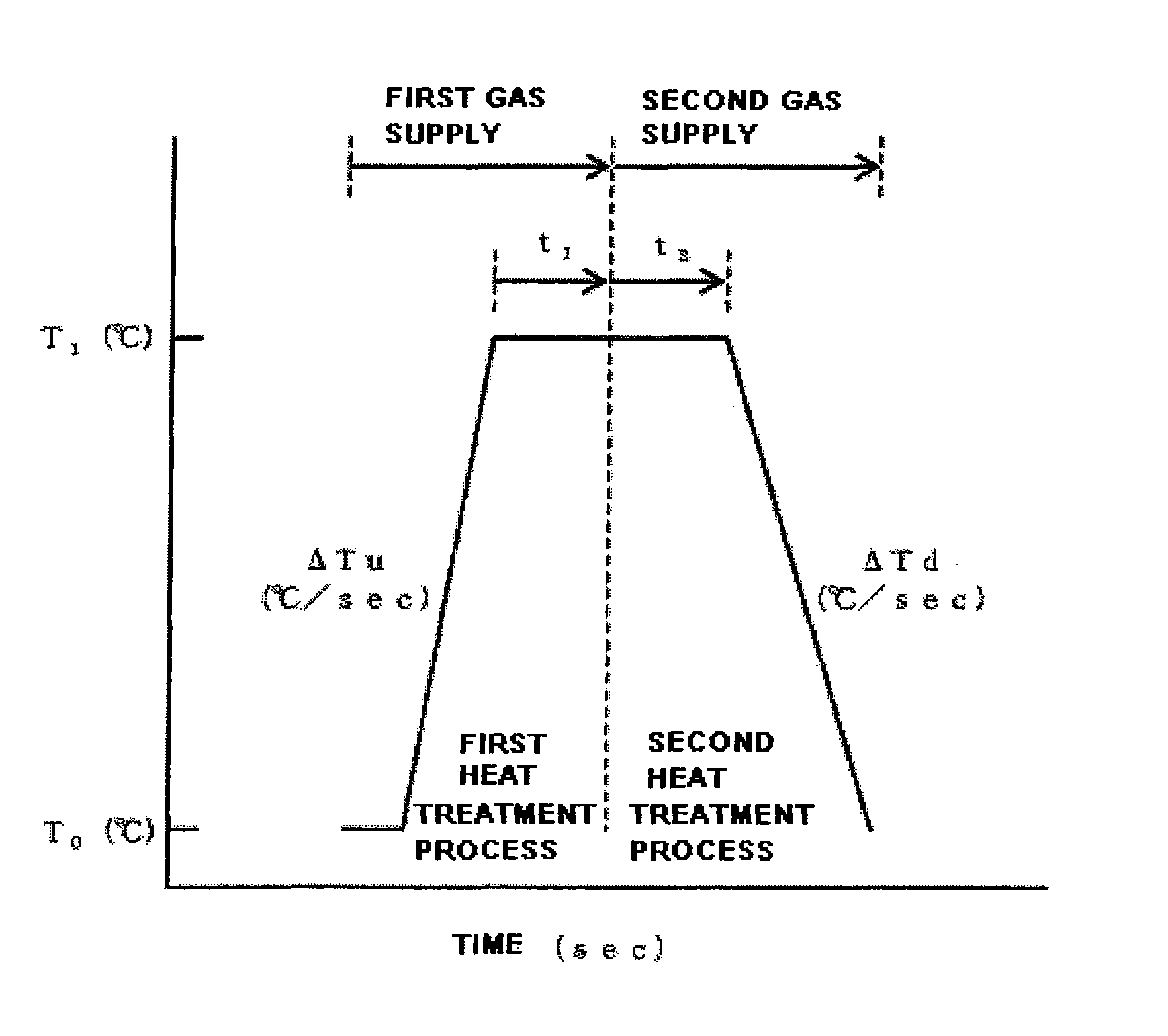
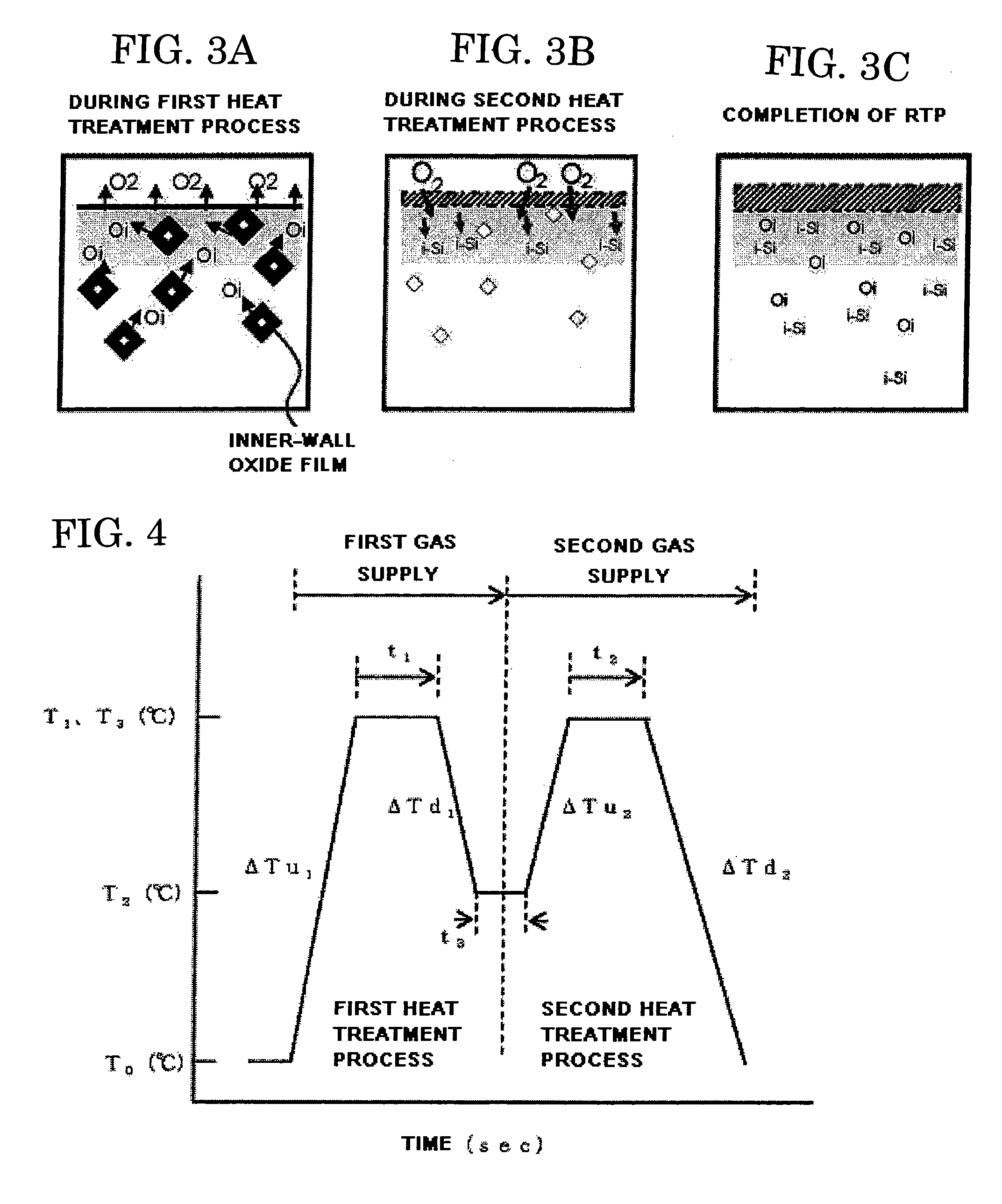
[0089]FIG. 4 is a schematic view for illustrating the production conditions in a rapid heating / cooling thermal process to be applied to the manufacturing method for a silicon wafer according to the second embodiment of the invention.

[0090]In the rapid heating / cooling thermal process according to the second embodiment of the invention, a first heat treatment process is performed while introducing a first gas, and a second heat treatment process is performed while stopping introducing the first gas and instead, introducin...

example 1

[0123]A silicon single crystal ingot having a P type, a crystal plane direction (001), a concentration of oxygen solid solution [Oi] of 1.2×10¹⁸ atoms / cm3 (calculated based on a conversion factor of Old ASTM standards in 1970-1979 Edition), and a resistance of from 23 to 25 Ω / cm was produced by CZ process.

[0124]At the time of production, nitrogen doping treatment was performed by putting a silicon wafer coated with a silicon nitride film in a crucible and a pull rate V was adjusted to 1.2 mm / min on average. At the same time, the pull rate and a temperature gradient G at 1300° C. in the direction of a crystal axis were controlled to control a V / G ratio in order to prevent generation of dislocation clusters during the growth of a silicon single crystal.

[0125]The resulting silicon single crystal ingot was then sliced into wafers by a wire saw and subjected to beveling, lapping, etching, and polishing to obtain a double-side polished silicon wafer having a diameter of 300 mm.

[0126]Then,...


PUM

PropertyMeasurementUnit
temperatureaaaaaaaaaa

Abstract

In a manufacturing method for a silicon wafer, a first heat treatment process is performed on the silicon wafer while introducing a first gas having an oxygen gas in an amount of 0.01 vol. % or more and 1.00 vol. % or less and a rare gas, and a second heat treatment process is performed while stopping introducing the first gas and introducing a second gas having an oxygen gas in an amount of 20 vol. % or more and 100 vol. % or less and a rare gas. In the first heat treatment process, the silicon wafer is rapidly heated to first temperature of 1300° C. or higher and a melting point of silicon or lower at a first heating rate, and kept at the first temperature. In the second heat treatment process, the silicon wafer is kept at the first temperature, and rapidly cooled from the first temperature at a first cooling rate.

Description

BACKGROUND OF THE INVENTION[0001]1. Field of the Invention[0002]The present invention relates to a manufacturing method for a silicon wafer to be used as a substrate of semiconductor devices.[0003]2. Description of Related Art[0004]With trends toward high integration of semiconductor devices in recent years, requirement for quality of a silicon wafer to be used as a substrate of such semiconductor devices is becoming severer. In particular, there is an eager demand for the development of a silicon wafer having less grown-in defects in the device active region.[0005]A technique of performing heat treatment on a silicon wafer is well known as a process for reducing such grown-in defects.[0006]As one example of such a technique, there is a technique of heat treating a silicon wafer at a temperature of 1000° C. or higher and 1350° C. or lower for 50 hours or less in a hydrogen and / or inert gas atmosphere, followed by oxidation heat treatment at a temperature range of 800° C. or higher a...

Claims


Application Information

Patent Timeline
Patent Type & Authority Patents(United States)
IPC IPC(8): H01L21/20
CPCC30B15/00H01L21/3225C30B33/02C30B29/06H01L21/20
Inventor ISOGAI, HIROMICHISENDA, TAKESHITOYODA, EIJIMURAYAMA, KUMIKOIZUNOME, KOJIMAEDA, SUSUMUKASHIMA, KAZUHIKO
Owner GLOBALWAFERS JAPAN
Why Eureka
Try Eureka