
Direct nanoscale patterning of metals using polymer electrolytes

a technology of polymer electrolytes and nano-scale patterns, applied in microstructural technology, microstructured devices, electrochemical machining apparatuses, etc., can solve problems such as inability to match approaches, and achieve high throughput patterning, excellent reproducibility, and robust and commercially attractive manufacturing pathways.

Inactive Publication Date: 2011-08-16
THE BOARD OF TRUSTEES OF THE UNIV OF ILLINOIS
View PDF13 Cites 19 Cited by
  • Summary
  • Abstract
  • Description
  • Claims
  • Application Information

AI Technical Summary

Benefits of technology

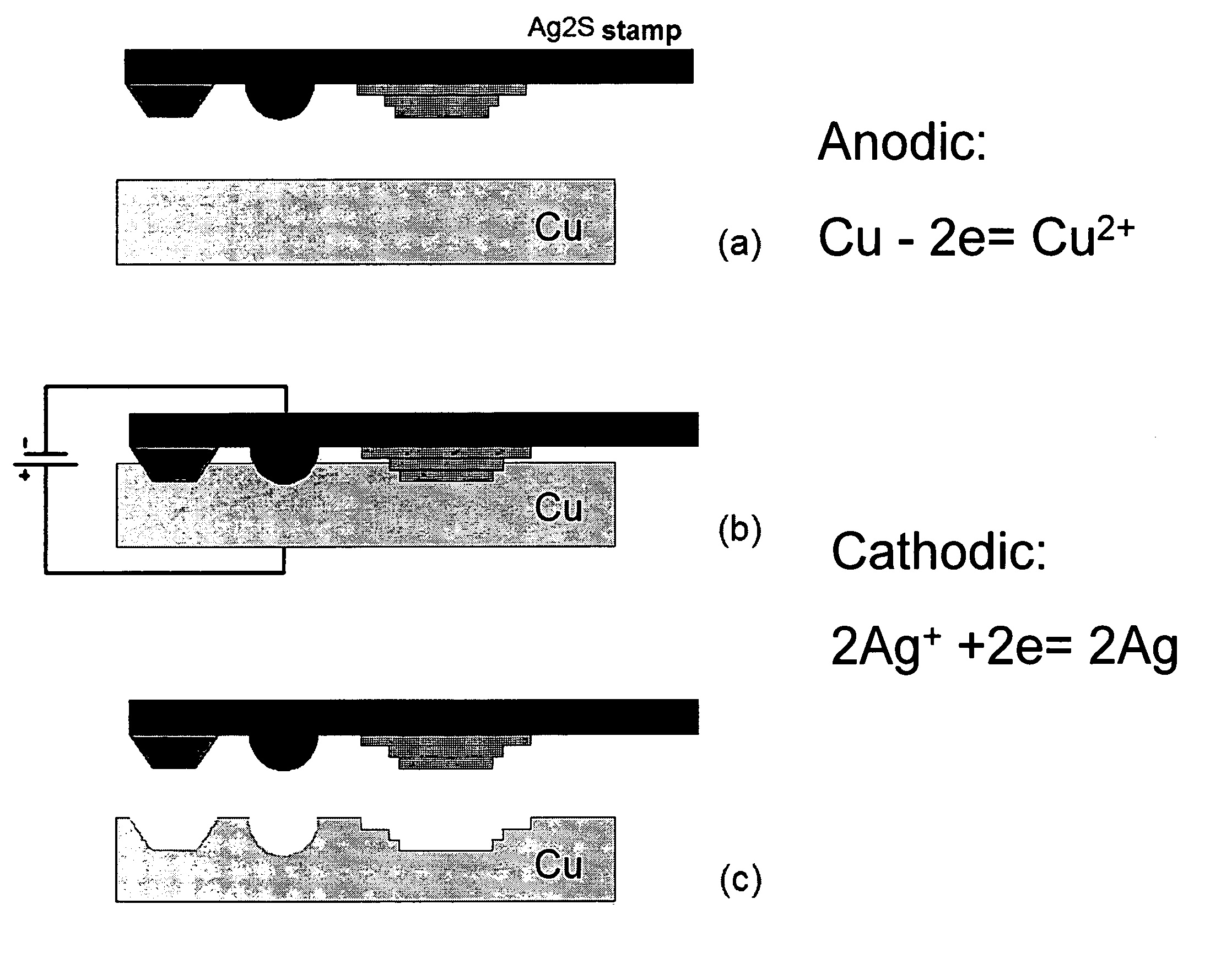
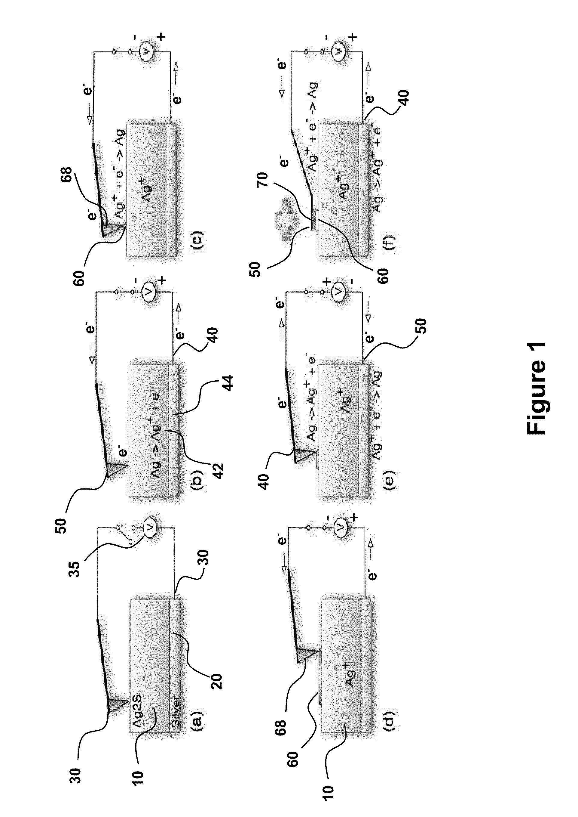
[0010]Provided are electrochemical fabrication platform for making structures, arrays of structures and functional devices having selected nanosized and / or microsized physical dimensions, shapes and spatial orientations. Methods, systems and system components disclosed herein use an electrochemical stamping tool for generating patterns of relief and / or recessed features exhibiting excellent reproducibility, pattern fidelity and resolution on surfaces of solid state ionic conductors and in metal layers. Electrochemical stamping tools of the present invention are capable high throughput patterning of large substrate areas and, thus, enable a robust and commercially attractive manufacturing pathway to a range of functional systems and devices including nano- and micro-electromechanical systems, sensors, energy storage devices and integrated electronic circuits. Further, nanopatterning and micropatterning methods and systems of the present invention are compatible with a wide range of materials, including metals, metal alloys, ionic conductors and superionic conductors, and processing conditions, including room temperature (below about 30° C.) processing.
[0011]Advantages of the processes provided herein, such as a electrochemical stamping with solid-state ionic stamps include high-throughput and high-rate processes. The stamping processes provided herein are compatible with simultaneous production of multiple spatial features that is readily scaled-up to high-production rates for massive manufacturing. In addition, the processes provide access to large-area patterning that conventional approaches cannot match. The solid state ionic conductors provide high resolution and dimensional fidelity not achievable with liquid-based processes. The processes provided herein are optionally reprogrammable in that an ionic stamp can be programmed and reprogrammed with different nanopatterns for processes such as nano imprint lithography (see www.nanonex.com for information on imprint lithography), molding, transfer printing, etc. With appropriate solid electrolytes, this process can be used to directly produce a desired metallic mask, saving steps in the conventional photolithography process.

Problems solved by technology

In addition, the processes provide access to large-area patterning that conventional approaches cannot match.

Method used


Image

  • Direct nanoscale patterning of metals using polymer electrolytes
  • Direct nanoscale patterning of metals using polymer electrolytes
  • Direct nanoscale patterning of metals using polymer electrolytes

Examples


example 1

Reprogrammable Patterning of Functional Nanostructures Using Superionic Conduction

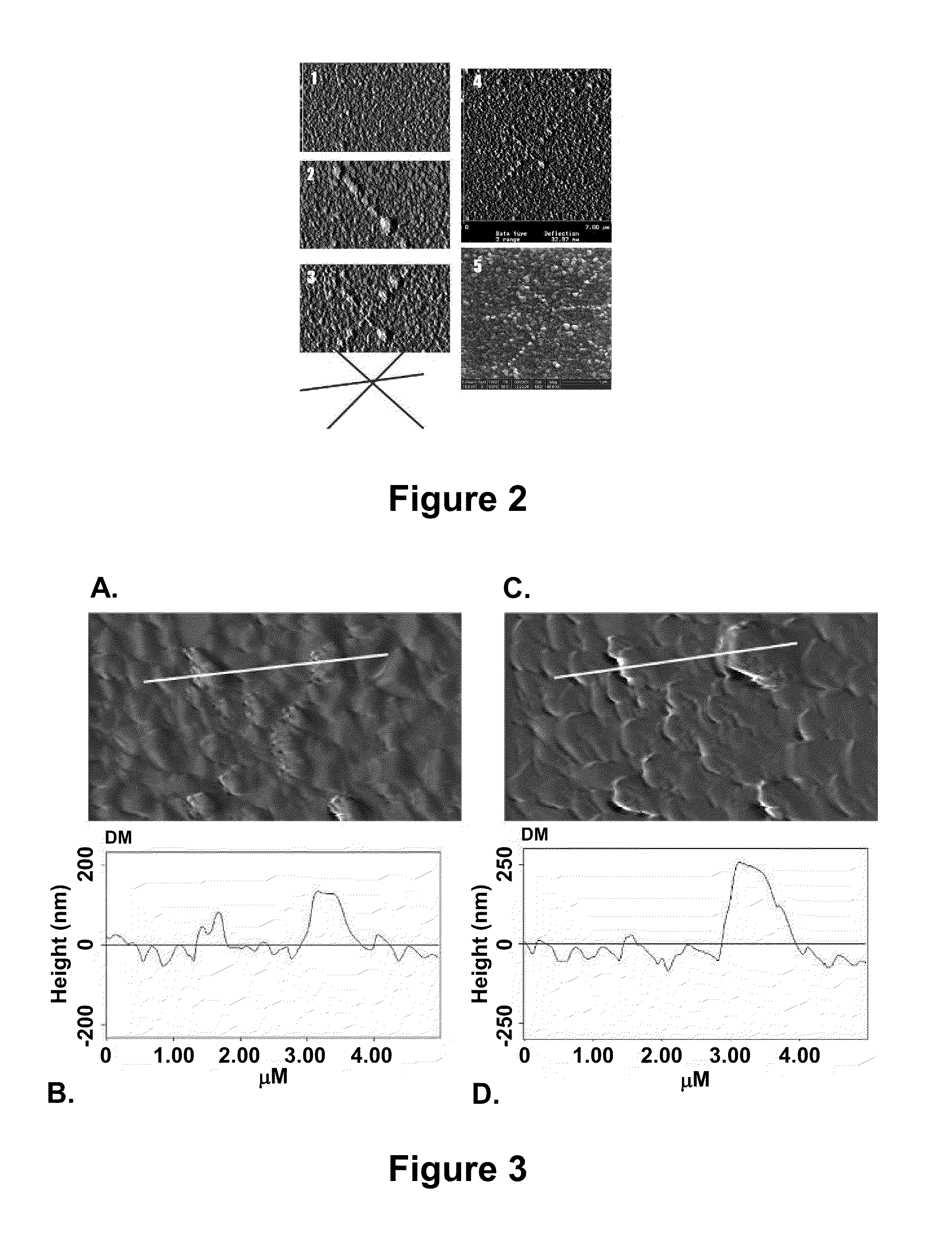
[0120]Reprogrammable and reconfigurable active nanostructures and processes influence the functional materials and devices to obtain enhanced energy conversion and chemical sensing. These experiments address outstanding issues in molecular-scale nanofabrication with superionic conduction by: (1) Addressing and explaining the underlying mechanisms of nanoscale charge, mass and energy transport, and reaction kinetics involved in nanostructure formation as a result of ionic conduction in solids; (2) Identifying the factors controlling growth rate and shape fidelity in the grown structures and exploiting this knowledge to develop a highly scalable and reprogrammable, in-parallel transfer stamping process; (3) Exploiting the new capability of programmable and reconfigurable patterning of nanostructures to actively regulate ionic transport and electron flow towards enhanced energy conversion and chemical sen...

example 2

Direct Nanopatterning with Solid Ionic Stamping

[0139]FIG. 15A is an SEM image of an Ag2S solid state ionic conductor stamp used for electrochemical stamping and FIG. 15B an SEM image of the corresponding pattern etched in Ag metal.

[0140]This example discloses an embodiment for generating sub-hundred nanometer features that integrates and extends the concepts of nanoimprint lithography and electrochemical micromachining. Realized by the mass transport property of solid-state ionic conductors and their dimensional integrity, this technique provides simplicity and high throughput of single-step pattern generation while keeping high feature resolution and reproducibility. In an embodiment, the solid-state ionic conductor is silver sulfide and is made into a stamping tool on which calibration features are defined to verify the lateral resolution capabilities of this technique. Stamping is achieved under various driving potentials and sub-hundred-nanometer lateral resolution is obtained. ...

example 3

Electrochemical Stamping

[0162]The invention disclosed herein provides a unique and new capability to pattern metals with sub-100 nm resolution in a high-through put stamping process. For example, FIG. 22 shows arrays of patterns can be etched in metal. Depending on manufacturing considerations, such a 5×5 array may be created using single step electrochemical stamping, or alternatively, the metal may be repeatedly stamped to obtain the array. FIG. 23 shows the stamps of the present invention provide structures having sub-100 nm resolution. For example, multiple distinct lines or channels are generated that are separated by 50 nm and the lateral resolution is 60 nm. In an embodiment, the process is a solid-state, room temperature process that is highly compatible with a large variety of process technologies. Although the examples provided herein utilize silver, different ionic crystals for other materials, including but not limited to copper, and gold, can be similarly used, to obtai...


PUM

PropertyMeasurementUnit
surface areaaaaaaaaaaa
frequencyaaaaaaaaaa
temperatureaaaaaaaaaa

Abstract

Disclosed herein are electrochemical fabrication platforms for making structures, arrays of structures and functional devices having selected nanosized and / or microsized physical dimensions, shapes and spatial orientations. Methods, systems and system components use an electrochemical stamping tool such as solid state polymeric electrolytes for generating patterns of relief and / or recessed features exhibiting excellent reproducibility, pattern fidelity and resolution on surfaces of solid state ionic conductors and in metal. Electrochemical stamping tools are capable high throughput patterning of large substrate areas, are compatible with commercially attractive manufacturing pathways to access a range of functional systems and devices including nano- and micro-electromechanical systems, sensors, energy storage devices, metal masks for printing, interconnects, and integrated electronic circuits.

Description

CROSS-REFERENCE TO RELATED APPLICATIONS[0001]This application claims the benefit of U.S. Provisional Application No. 60 / 938,934 filed May 18, 2007 and is a continuation-in-part application of U.S. patent application Ser. No. 11 / 376,908 filed Mar. 16, 2006 and PCT / US2007 / 064132 filed Mar. 16, 2007, which claims the benefit of U.S. patent application Ser. No. 11 / 376,908, each of which are hereby incorporated by reference in their entireties to the extent they are not inconsistent with the disclosure herein.STATEMENT REGARDING FEDERALLY SPONSORED RESEARCH OR DEVELOPMENT[0002]This invention was made, at least in part, with United States governmental support awarded by National Science Foundation under contract number DMI-0328162. The United States government has certain rights in this invention.BACKGROUND OF THE INVENTION[0003]The use of solid state ionic conductors allows for nano-scale patterning and stamping by highly localized electrochemical etching and deposition. When an electric...

Claims


Application Information

Patent Timeline
Patent Type & Authority Patents(United States)
IPC IPC(8): C25D5/02C25D17/00
CPCB23H3/00C25D1/006B81C1/0046C25D5/02C25D11/22H01L21/32134H05K3/07C25D17/007C25D1/00B23H3/04B81C2201/0154B82Y30/00G01Q80/00H05K2203/0108H05K2203/0117C25F3/14C25F7/00
Inventor FANG, NICHOLAS X.FERREIRA, PLACID M.HSU, KENG HAOSCHULTZ, PETER LEEJACOBS, KYLE E.KUMAR, ANIL
Owner THE BOARD OF TRUSTEES OF THE UNIV OF ILLINOIS
Learn More