
Thin film transistor, thin film transistor substrate, processes for producing the same, liquid crystal display using the same, and related devices and processes; and sputtering target, transparent electroconductive film formed by use of this, transparent electrode, and related devices and processes

a thin film transistor and substrate technology, applied in the direction of conductive materials, solid-state devices, conductive layers on insulating supports, etc., can solve the problems of pixel inferiority, pixel inferiority based on etching residues, and failure of etching, so as to reduce the light transmittance of laminated metal thin films

Inactive Publication Date: 2011-10-18
IDEMITSU KOSAN CO LTD
View PDF59 Cites 32 Cited by
  • Summary
  • Abstract
  • Description
  • Claims
  • Application Information

AI Technical Summary

Benefits of technology

[0298]In this case, the film thickness of the metal thin film made mainly of Al or Ag is from 1 to 20 nm. The film thickness is preferably from 5 to 15 nm, more preferably from 5 to 10 nm. If the film thickness is 1 nm or less, the laminated metal film does not become a “thin film” but may become a sea-island structure. Thus, the advantageous effects of the invention may not be obtained. On the other hand, if the film thickness of the metal thin film is 20 nm or more, the light transmittance of the laminated metal thin film may be lowered. As a result, an effect may be actually produced on the “transparency” of the transparent electroconductive film formed to be overlapped thereon.
[0299]In the invention, the transparent electroconductive film made of a metal oxide and the metal thin film made mainly of Al or Ag are frequently laminated on each other; the meaning of the wording “being laminated” includes a case where (not the whole of the transparent electroconductive film, which is made of the metal oxide, but) a part of the transparent electroconductive film contacts the metal thin film. Examples of the electrode structure in this case include a case where the transparent electroconductive film contacts a part of the metal thin film having a width of, e.g., 20 μm and covers the whole of the metal thin film. In other words, the two overlap with each other as viewed in a plan view thereof, but only parts thereof contact each other as viewed in a sectional view thereof.
[0300]In such a case, the thickness of the metal thin film is from 20 to 500 nm, more preferably from 30 to 300 nm, even more preferably from 50 to 200 nm. If the film thickness is 20 nm or less, the effect of decreasing the resistance may be small. On the other hand, if the film thickness is 500 nm or more, a level difference in the thin film is large so that the contact thereof with the transparent electroconductive film may become poor.
[0301]The width of the metal thin film can be appropriately selected, and is, for example, from 1 to 100 μm. This value is preferably from 5 to 50 μm, more preferably from 10 to 30 μm.
[0302]If the width of the metal thin film is 1 μm or less, the resistance-decreasing effect may be too small. On the other hand, if the width of the metal thin film is 100 μm or more, the light transmittance (numerical aperture) may decline. However, the width is not limited to this range in the case of using the lamination of the metal thin film and the transparent electroconductive film as a reflecting electrode.
[0304]A. Invention of a Process for Producing a Thin Film Transistor Substrate

Problems solved by technology

This mixture frequently causes problems that etching failures (electric conduction to an adjacent electrode, the narrowing of the pixel electrode by overetching, pixel inferiority based on etching residues, and so on) are generated.
About a target of ITO, black nodules are generated on the surface of the target when a film is continuously formed over a long time, so that over discharge is caused or foreign substances are generated to cause pixel inferiority.
These also become problems with frequency.
However, the addition of water or hydrogen at the time of the film-formation frequently causes a decline in the adhesiveness to the underlying substrate, or causes the surface of ITO to be reduced, thereby generating a large amount of nodules.
However, it appears that if the time for etching the ITO film is long or defects portions, such as impurities or foreign substances incorporated during the deposition of Al, are present in the Al film, the above-mentioned Al-oxidizing effect does not act sufficiently by local cell reaction.
However, even if the ITO film is made amorphous, elution of Al is not completely prevented since an HCl—HNO3—H2O-based etching solution is used.
Thus, a highly definited liquid crystal display is not easily realized.
This is because the pure Al or Al alloy has a low electric resistance.
It has been therefore considered that it is difficult to obtain a favorable contact resistance in any TFT array substrate having a structure wherein a first conductor made of pure Al or Al alloy directly contacts a second conductor made of a transparent electroconductive film of ITO, IZO or the like through a contact hole made in an insulation film.
However, it is considered that if the time for etching the ITO film is long or defects portions, such as impurities or foreign substances incorporated during the deposition of Al, are present in the Al film, the above-mentioned Al-oxidizing effect does not act sufficiently by local cell reaction.
However, even if the ITO film is made amorphous, elution of Al is not completely prevented since an HCl—HNO3—H2O-based etching solution is used.
Thus, a highly definited liquid crystal display is not easily realized.
In the case of using Al wirings in this way, it is unavoidable to use a barrier metal; it is therefore necessary to form the barrier metal into a film and etch the film.
As a result, it is feared that the production process is made complicated.
However, it is presumed that it is very difficult to make the above-mentioned contact resistance small.
Moreover, there arise a problem that the transmittance of the pixel electrode declines, and other problems.

Method used


Image

  • Thin film transistor, thin film transistor substrate, processes for producing the same, liquid crystal display using the same, and related devices and processes; and sputtering target, transparent electroconductive film formed by use of this, transparent electrode, and related devices and processes
  • Thin film transistor, thin film transistor substrate, processes for producing the same, liquid crystal display using the same, and related devices and processes; and sputtering target, transparent electroconductive film formed by use of this, transparent electrode, and related devices and processes
  • Thin film transistor, thin film transistor substrate, processes for producing the same, liquid crystal display using the same, and related devices and processes; and sputtering target, transparent electroconductive film formed by use of this, transparent electrode, and related devices and processes

Examples


example 1-1

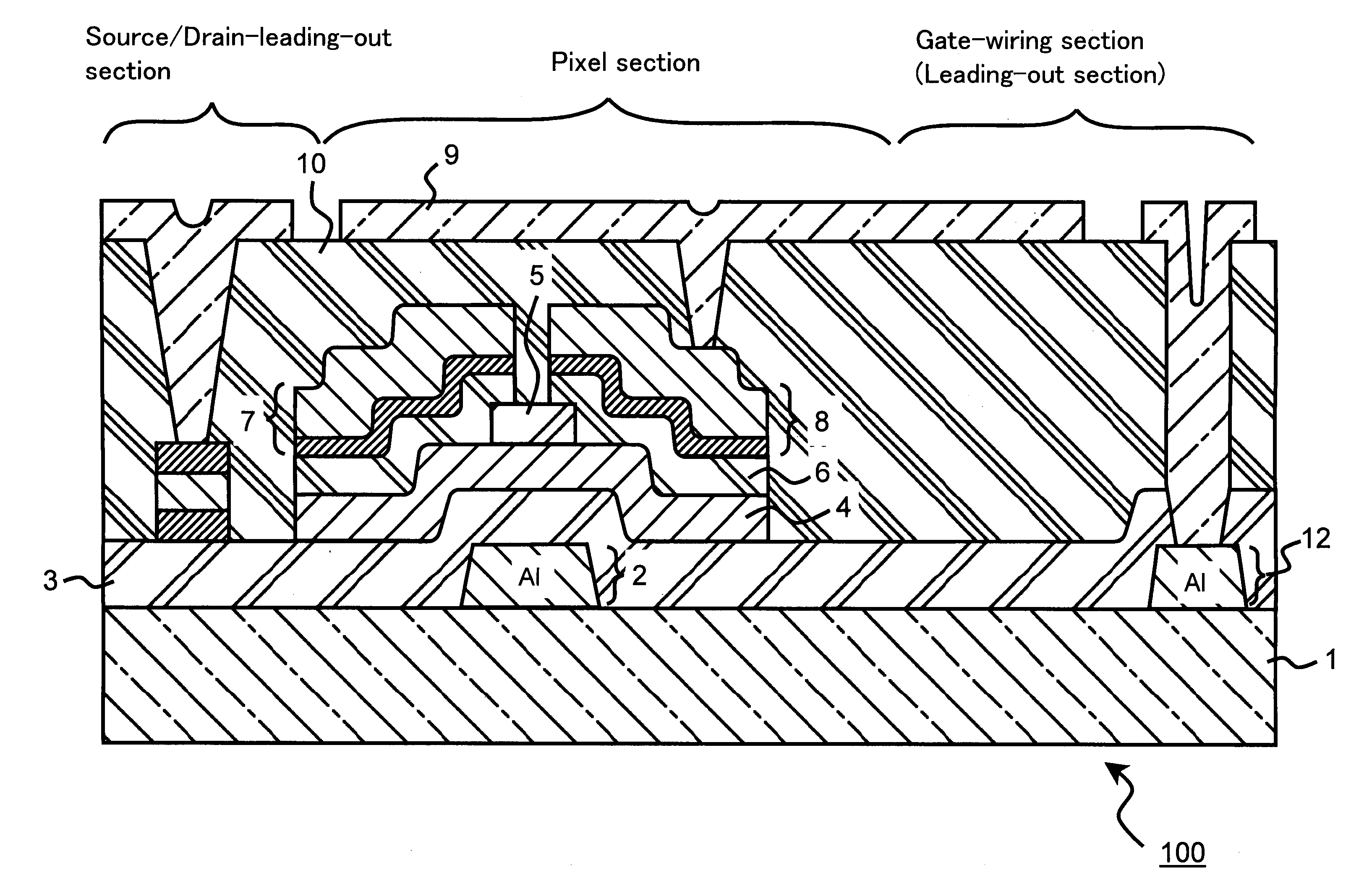
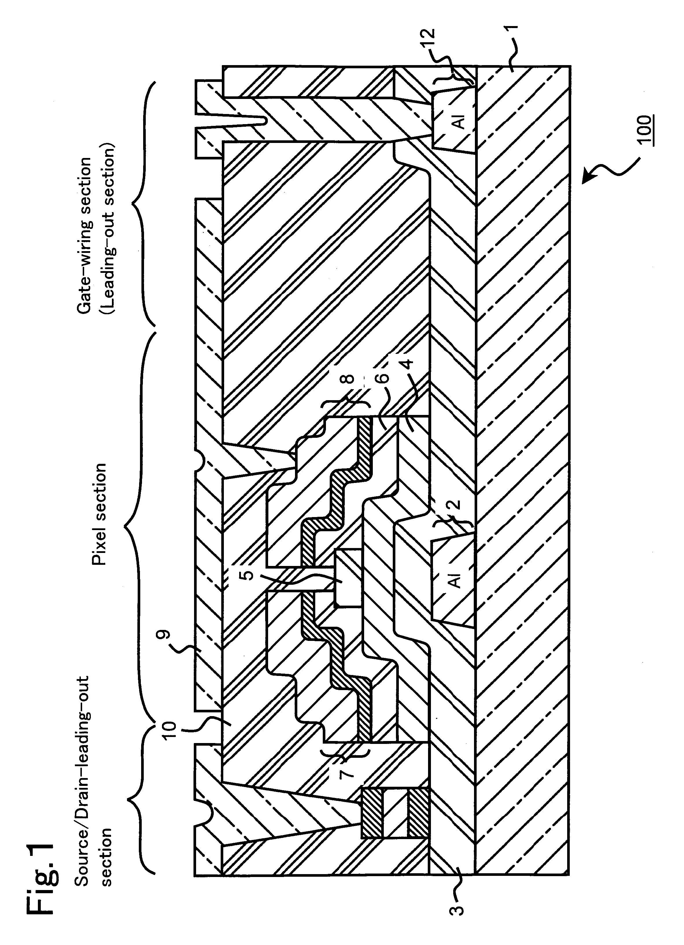
[0466]FIG. 1 illustrates a sectional view of a vicinity of an α-SiTFT (amorphous silicon thin film transistor) active matrix substrate 100 in the Example 1-1. Metallic Al was deposited onto a light-transmissible glass substrate 1 by high-frequency sputtering so as to have a film thickness of 1500 Å. This glass substrate 1 corresponds to one example of the transparent substrate described in the claims.

[0467]Next, the deposited Al was etched into a shape illustrated in FIG. 1 by photo-etching using a phosphoric acid / acetic acid / nitric acid / water (the ratio by volume=12 / 6 / 1 / 1)-based aqueous solution as an etchant to form a gate electrode 2 and a gate electrodewiring 12.

[0468]Next, a silicon nitride film (hereinafter, denoted as a SiN film in some cases), which would be a gate insulation film 3, was deposited on the glass substrate 1, the gate electrode 2 and the gate electrode wiring 12 by glow discharge CVD, so as to have a film thickness of 3000 Å. Subsequently, an α-Si:H (i) film 4 ...

example 1-2

[0483]An α-SiTFT active matrix substrate 100 in Example 1-2 is different from the α-SiTFT active matrix substrate 100 in Example 1-1 only in the composition of the transparent electroconductive film 9, and the structure thereof is substantially the same as in FIG. 1. Accordingly, the α-SiTFT active matrix substrate 100 of Example 1-2 will also be described using FIG. 1.

[0484]As illustrated in FIG. 1, metallic Al was deposited onto a light-transmissible glass substrate 1 by high-frequency sputtering so as to have a film thickness of 1500 Å. Next, the deposited Al was etched into a shape illustrated in FIG. 1 by photo-etching using a phosphoric acid / acetic acid / nitric acid / water (the ratio by volume=12 / 6 / 1 / 1)-based aqueous solution as an etchant to form a gate electrode 2 and a gate electrode wiring 12. This glass substrate 1 corresponds to one example of the transparent substrate described in the claims.

[0485]Next, a silicon nitride film (hereinafter, denoted as a SiN film in some ca...

example 1-3

[0500]An α-SiTFT active matrix substrate 100 in Example 1-3 is different from the α-SiTFT active matrix substrate 100 in Examples 1-1 to 1-2 only in the composition of the transparent electroconductive film 9, and the structure thereof is substantially the same as in FIG. 1. Accordingly, the α-SiTFT active matrix substrate 100 of Example 1-3 will also be described using FIG. 1.

[0501]A metallic Al (alloy) (the composition weight %: Al / Ni=99 / 1) was deposited onto a light-transmissible glass substrate 1 by high-frequency sputtering so as to have a film thickness of 2500 Å. Next, the deposited Al was etched into the same shapes as the gate electrode 2 and the gate electrode wiring 12 in FIG. 1 by photo-etching using a phosphoric acid / acetic acid / nitric acid / water (the ratio by volume=9 / 6 / 1 / 2)-based aqueous solution as an etchant to form a gate electrode 2 and a gate electrode wiring 12. This glass substrate 1 corresponds to one example of the transparent substrate described in the claim...


PUM

PropertyMeasurementUnit
temperatureaaaaaaaaaa

Abstract

Provided are a thin film transistor substrate having a transparent electroconductive film in which residues and so on resulting etching are hardly generated; a process for producing the same; and a liquid crystal display using this thin film transistor substrate.A thin film transistor substrate, comprising a transparent substrate,a source electrode formed over the transparent substrate, a drain electrode formed over the transparent substrate, and a transparent pixel electrode formed over the transparent substrate, wherein the transparent pixel electrode is a transparent electroconductive film which is made mainly of indium oxide, and further comprises one or two or more oxides selected from tungsten oxide, molybdenum oxide, nickel oxide and niobium oxide, and the transparent pixel electrode is electrically connected to the source electrode or the drain electrode; a process for producing the same; and a liquid crystal display using this thin film transistor substrate.

Description

TECHNICAL FIELD[0001]First Group: Field[0002]The invention of the first group relates to a thin film transistor substrate for driving the liquid crystal of a liquid crystal display. The invention also relates to a process for producing the thin film transistor substrate, and a liquid crystal display using the thin film transistor substrate.[0003]An abbreviation of a thin film transistor is used to call a thin film transistor substrate a TFT substrate in some cases.[0004]Second Group: Field[0005]The invention of the second group relates to a process for producing a liquid crystal display, using an amorphous silicon thin film transistor (α-SiTFT) or a polysilicon thin film transistor (p-SiTFT). More specifically, the invention relates to a liquid crystal display enabling to reduce the contact resistance between a pixel electrode pattern and source / drain wirings, and the contact resistance between the following: wiring metals of a gate wiring leading-out section and source / drain electr...

Claims


Application Information

Patent Timeline
Patent Type & Authority Patents(United States)
IPC IPC(8): C23C14/08C23C14/34G02F1/1343G02F1/1362G02F1/1368H01B5/14H01L21/28H01L21/285H01L21/308H01L21/3205H01L21/336H01L21/77H01L27/12H01L29/45H01L29/786
CPCC04B35/01H01L27/124C23C14/08C23C14/3414G02F1/13439H01L23/53219H01L23/53247H01L27/12H01L29/458H01L29/4908H01L29/66765H01L29/78696C04B2235/3227C04B2235/3229C04B2235/3251C04B2235/3256C04B2235/3258C04B2235/3279C04B2235/3284C04B2235/3286C04B2235/3287C04B2235/3289C04B2235/5436C04B2235/5445C04B2235/77G02F1/136227G02F1/1368H01L2924/0002C04B2235/3224H01L2924/00H01L27/1214
Inventor INOUE, KAZUYOSHITOMAI, SHIGEKAZUMATSUBARA, MASATO
Owner IDEMITSU KOSAN CO LTD
Learn More