Driver circuit usable for display panel

a driver circuit and display panel technology, applied in pulse manipulation, instruments, pulse technique, etc., can solve the problems of increasing the overall consumption of an integrated circuit chip which is integrated with a plurality of driver circuits, and it is difficult to realize a driver circuit usable for a display panel

Active Publication Date: 2011-10-25
LAPIS SEMICON CO LTD
View PDF9 Cites 13 Cited by
  • Summary
  • Abstract
  • Description
  • Claims
  • Application Information

AI Technical Summary

Benefits of technology

[0012]An object of the present invention is to provide a driver circuit usable for a display panel that can generate an output signal at a high slew rate and decrease electric consumption while avoiding increase of the circuit area.
[0016]According to the first aspect of the present invention, the driver circuit has the following effects (a) to (c).
[0017](a) The driver circuit includes the superimposing stage which deeply turns on the output transistors, respectively and superimposing electric currents on first and second differential amplifier stages only at the time when the output signal changes. Thus, the driver circuit can generate the output signal at a high slew rate without increasing stationary electric current consumption.
[0019](c) The driver circuit having the auxiliary output stage can decrease electric leakage currents flowing to the output transistors of the output stages.
[0021]The driver circuit according to the second aspect has effects similar to the first aspect of the present invention. The driver circuit can control charging and discharging of an external load without providing the external switch. The output stage to which the stop signals are supplied are provided with the driver circuit, so that generating timing of the output signal can be arbitrarily changed. The driver circuit is effective for driving a LCD source driver etc. that especially need a high-impedance performance.

Problems solved by technology

However, the LCD source driver has a plurality of the driver circuits whose number corresponds to the number of outputs and the electric currents flowing to the differential input stage 50 are increased constantly, thus largely increasing overall consumption of an integrated circuit chip which is integrated with a plurality of the driver circuits.
Therefore, it is technically difficult to realize a driver circuit usable for a display panel that can generate an output voltage at a sufficient high slew rate.

Method used


Image

  • Driver circuit usable for display panel
  • Driver circuit usable for display panel
  • Driver circuit usable for display panel

Examples


first embodiment

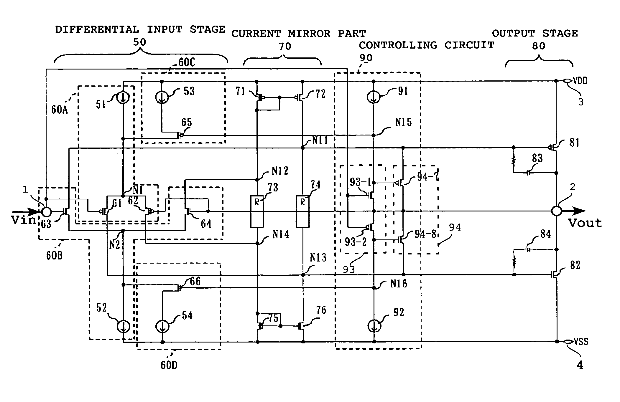
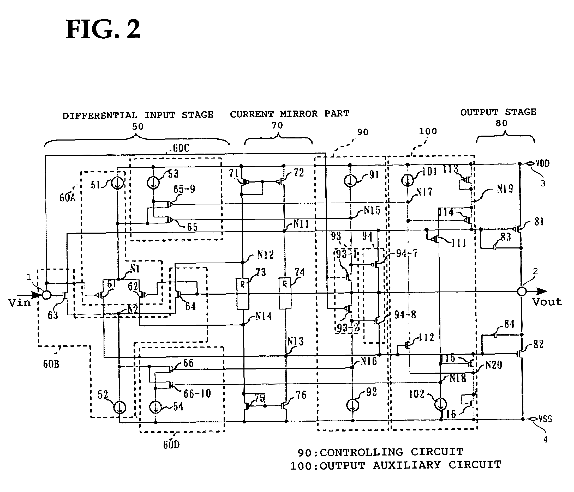
[0032]FIG. 2 is a circuit diagram showing a driver circuit that is a first embodiment of the present invention.

[0033]This driver circuit operational at a high slew rate includes a differential input stage 50, a current mirror part 70, a push-pull type output stage 80, a first auxiliary current source part 60C, a second auxiliary current source part 60D, a controlling circuit 90, and a power output auxiliary circuit 100. The differential input stage 50 has a first differential input stage 60A which is a first conductive type (e.g., a p-type differential input stage) and a second differential input stage which is a second conduction type (e.g., an N-type differential input stage).

[0034]The p-type differential input stage 60A has a first current source 51, a first transistor (e.g., a PMOS transistor) 61, and a second transistor (e.g., a PMOS transistor) 62. The first current source 51 is connected to a power-supply terminal 3 from which a power-supply voltage of VDD level is supplied a...

second embodiment

[0066]FIG. 4 is circuit diagram showing a driver circuit that is a second embodiment of the present invention. Components in FIG. 4 which operate in the same manner as those in FIG. 2 are denoted by the same reference numerals.

[0067]In the driver circuit of the second embodiment, a P-type output stop part 120 and an N-type output stop part 130 are added to the first embodiment.

[0068]The output stop parts 120 and 130 are so configured that electrical potentials at nodes N11 and N13 are fixed on the basis of complementary control signals DSB (e.g., VDD) and XDSB (e.g., VSS). The output stop parts 120 and 130 are also so configured that a PMOS transistor 81 and an NMOS transistor 82 of an output stage 80 are turned off at the same time.

[0069]The P-type output stop part 120 has PMOS transistors 121, 122, 123, and 124 whose gate are controlled by the control signal DSB and a PMOS transistor 125 whose gate is controlled by the control signal XDSB having a reversed phase. Source and drain ...

third embodiment

[0076]FIG. 5 is a circuit diagram showing a driver circuit that is a fourth embodiment of the present invention. Components in FIG. 5 which operate in the same manner as those in FIG. 2 are denoted by the same reference numerals.

[0077]In the driver circuit of the third embodiment, the PMOS transistor 65-9 and the NMOS transistor 66-10 are deleted from the first auxiliary current source part 60C and the second auxiliary current source part 60D, respectively, both of which are included by the driver circuit of the first embodiment. The output auxiliary circuit 100 for controlling gated of the PMOS transistor 65-9 and the NMOS transistor 66-10 are also the output auxiliary circuit 100 of the first embodiment Other components are similar to those of the first embodiment.

[0078]The driver circuit of the third embodiment sequentially performs operations (1), (2), (3), and (5) which are described in the first embodiment and performs to a regular operation.

[0079]FIG. 3 is the wave form chart...


PUM


Abstract

A driver circuit usable for a display panel can generate an output signal in response to an input pulse signal supplied to only one input signal terminal thereof. The driver circuit includes a pulse generating circuit for generating an output signal at the output terminal. The pulse generating circuit has a first and second differential input stage for respectively driving a push-pull construction of output transistors in response to the input pulse signal supplied through the input signal terminal with respect to the push-pull output, whereby to simplify the circuitry, operate at a high slew rate, and decrease electric current consumption.

Description

1. FIELD OF THE INVENTION[0001]The present invention relates to a driver circuit usable for a display panel.2. DESCRIPTION OF THE RELATED ART[0002]A conventional driver circuit usable for a display panel such as a liquid crystal display (LCD) panel or an organic electroluminescence (EL) display panel is disclosed by, for example, Japanese Patent Kokai No. 2005-192260 (D1).[0003]A LCD panel disclosed by the document D1 is provided with an active matrix liquid crystal panel and a drive unit for driving the active matrix liquid crystal panel. The liquid crystal panel is formed from a matrix of liquid crystal display elements placed where plural scanning lines and plural data lines are intersected with each other. The drive unit has plural source drivers connected to the data lines and plural gate drivers connected to the scanning lines, both of which are controlled by a controller. Each of the source drivers includes plural driver circuits capable of providing output signals to the liq...

Claims


Application Information

Patent Timeline
Patent Type & Authority Patents(United States)
IPC IPC(8): G09G5/00
CPCG09G3/3688G09G3/20G09G3/30G09G3/36H03F3/46
Inventor SATOU, MASANORI
Owner LAPIS SEMICON CO LTD
Why Eureka
Try Eureka