Semiconductor substrate for solid-state image sensing device as well as solid-state image sensing device and method for producing the same

a solid-state image and sensor technology, applied in the direction of radiation controlled devices, final product manufacturing, sustainable manufacturing/processing, etc., can solve the problems difficult to completely avoid the epitaxial growth step metal contamination, and deterioration of the electrical properties of the solid-state image sensing device, so as to avoid the occurrence of defects in the device, reduce the effect of contaminating the semiconductor substrate with heavy metal, and suppress the diffusion of heavy metal

Active Publication Date: 2011-11-22
SUMCO CORP
View PDF11 Cites 95 Cited by
  • Summary
  • Abstract
  • Description
  • Claims
  • Application Information

AI Technical Summary

Benefits of technology

[0032]In the semiconductor substrate for solid-state image sensing device according to the invention, carbon-oxygen based precipitates having a high gettering ability can be formed by including solid-soluted carbon into CZ crystal or MCZ crystal and utilizing the heat treatment step in the production step of mounting a device on the semiconductor substrate.
[0033]Therefore, the gettering sink can be foamed just beneath the buried photodiode over a full thickness of the silicon substrate, so that the diffusion of heavy metal at the device production step is particularly suppressed to avoid the occurrence of defects in the device, and hence it is possible to provide a high quality solid-state image sensing device having good electric characteristics at a low cost.

Problems solved by technology

In this case, if a heavy metal is incorporated into the semiconductor substrate as an impurity, the electric properties of the solid-state image sensing device are deteriorated remarkably.
Recently, the metal contamination in the epitaxial growth step is attempted to be improved by replacing the constitutional material of the epitaxial growth furnace with a material having a corrosion resistance, but it is difficult to completely avoid the metal contamination at the epitaxial growth step.
On the other hand, in the latter case for the production step of the solid-state image sensing device, there is a fear of contaminating the semiconductor substrate with heavy metal at each of ion implantation step, diffusion step and oxidation heat treatment step among steps of producing the device.
In case of the above conventional gettering method, i.e. intrinsic gettering method, however, a multi-stage heat treatment step is required for previously forming the oxygen precipitate in the semiconductor substrate, so that there is feared the increase of the production cost.
Furthermore, it is required to conduct the heat treatment at a higher temperature for a long time, so that there is feared the new metal contamination to the semiconductor substrate.
In case of the extrinsic gettering method, since the back side damage or the like is formed in the back side, particles are generated from the back side at the device production step, which causes drawbacks such as formation of defective device and the like.
That is, in the gettering sink formed by the carbon ion implantation, there is a limit in the gettering effect.

Method used


Image

  • Semiconductor substrate for solid-state image sensing device as well as solid-state image sensing device and method for producing the same
  • Semiconductor substrate for solid-state image sensing device as well as solid-state image sensing device and method for producing the same
  • Semiconductor substrate for solid-state image sensing device as well as solid-state image sensing device and method for producing the same

Examples


examples

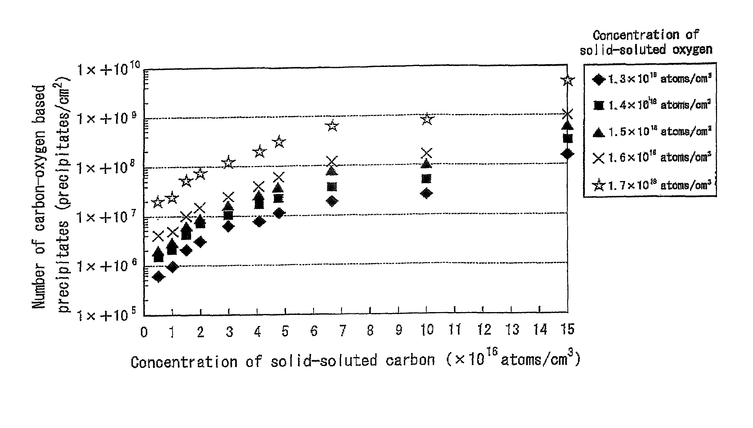
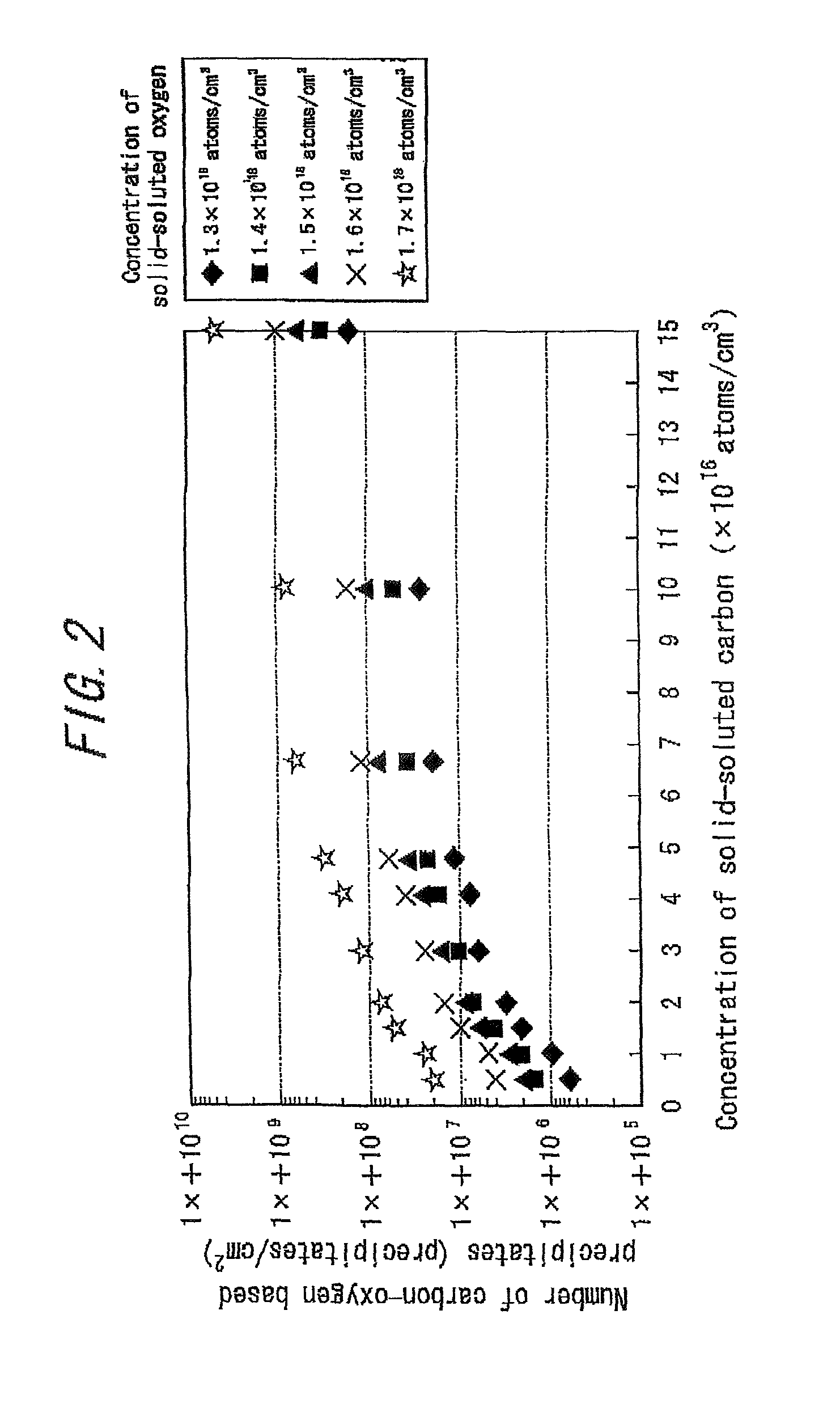
[0080]A heaped polysilicon as a starting material for silicon crystal is placed in a quartz crucible and a proper amount of graphite powder is applied onto the surface of the polysilicon, and then a CZ crystal added with carbon is prepared according to a Czochralski method (CZ method). Concentrations of solid-soluted carbon and solid-soluted oxygen in a silicon substrate cut out as a wafer from the CZ crystal are shown in Table 1. Then, the thus obtained silicon substrate is subjected to a surface contamination (contaminant: Fe, Cu, Ni and contamination concentration: 1×10¹³ atoms / cm2) by a spin coating method, and further subjected to a heat treatment under temperature conditions corresponding to a heat treatment in the production of a solid-state image sensing device.

[0081]With respect to a gettering ability of the silicon substrate, a contamination concentration of metals on the surface of the silicon substrate is measured by an atomic spectrophotometry and a gettering efficiency...


PUM


Abstract

There is provided a semiconductor substrate for solid-state image sensing device in which the production cost is lower than that of a gettering method through a carbon ion implantation and problems such as occurrence of particles at a device production step and the like are solved.Silicon substrate contains solid-soluted carbon having a concentration of 1×10¹⁶-1×10¹⁷ atoms / cm3 and solid-soluted oxygen having a concentration of 1.4×10¹⁸-1.6×10¹⁸ atoms / cm3.

Description

TECHNICAL FIELD[0001]This invention relates to a semiconductor substrate for a solid-state image sensing device as well as a solid-state image sensing device and a method for producing the same.RELATED ART[0002]The solid-state image sensing device is produced by forming circuits on a semiconductor substrate made of a silicon single crystal. In this case, if a heavy metal is incorporated into the semiconductor substrate as an impurity, the electric properties of the solid-state image sensing device are deteriorated remarkably.[0003]As a factor of incorporating the heavy metal as an impurity into the semiconductor substrate are, mentioned firstly a metal contamination at the production step of the semiconductor substrate and secondly a heavy metal contamination at the production step of the solid-state image-sensing device.[0004]As the former case, there is considered the contamination with heavy metal particles generated from a constituent material of an epitaxial growth furnace when...

Claims


Application Information

Patent Timeline
Patent Type & Authority Patents(United States)
IPC IPC(8): H01L31/14H01L31/18
CPCH01L21/3221H01L27/14603H01L31/186C30B15/04C30B29/06C30B33/02Y02P70/521Y02E10/50Y02P70/50H01L21/8258H01L27/146
Inventor KURITA, KAZUNARI
Owner SUMCO CORP
Why Eureka
Try Eureka