Method of treating semiconductor element

a technology of semiconductor elements and threshold voltages, applied in the direction of basic electric elements, semiconductor devices, electrical equipment, etc., can solve the problems of small influence of threshold voltage change and behavior problems, and achieve the effect of making the influence of threshold voltage relatively small

Inactive Publication Date: 2011-12-27
CANON KK
View PDF15 Cites 92 Cited by
  • Summary
  • Abstract
  • Description
  • Claims
  • Application Information

AI Technical Summary

Benefits of technology

[0009]In view of the above-mentioned problems, it is an object of the present invention to provide a method of treating a semiconductor element which enables compensation or restraining of undesirable change in threshold voltage.
[0027]With the present invention, the threshold voltage of the semiconductor element can be changed, and the threshold voltage shift due to factors such as manufacturing process history, time-dependent change, electrical stress, thermal stress, etc. can be compensated for or restrained. Furthermore, in the semiconductor element where the threshold voltage can be changed by the factors such as manufacturing process history, time-dependent change, electrical stress, thermal stress, etc., influence of such change in the threshold voltage can be made relatively small. In addition, characteristics (e.g. charge mobility, S value, etc.) other than the threshold voltage can be maintained at conditions equal to those before the process is performed.

Problems solved by technology

However, none of the above-mentioned references discloses a method of compensating for or restraining the threshold voltage shift that can be caused by various factors, or a method of making the influence of such change in the threshold voltage relatively small.
Such behaviors are problematic in a case where a load such as an organic light-emitting diode is connected to the TFT and a current to be supplied to the load is to be controlled by a gate voltage of the TFT.

Method used


Image

  • Method of treating semiconductor element
  • Method of treating semiconductor element
  • Method of treating semiconductor element

Examples


examples

[0080]Now, examples of the present invention will be described. The present invention is not to be limited by the following examples.

first example

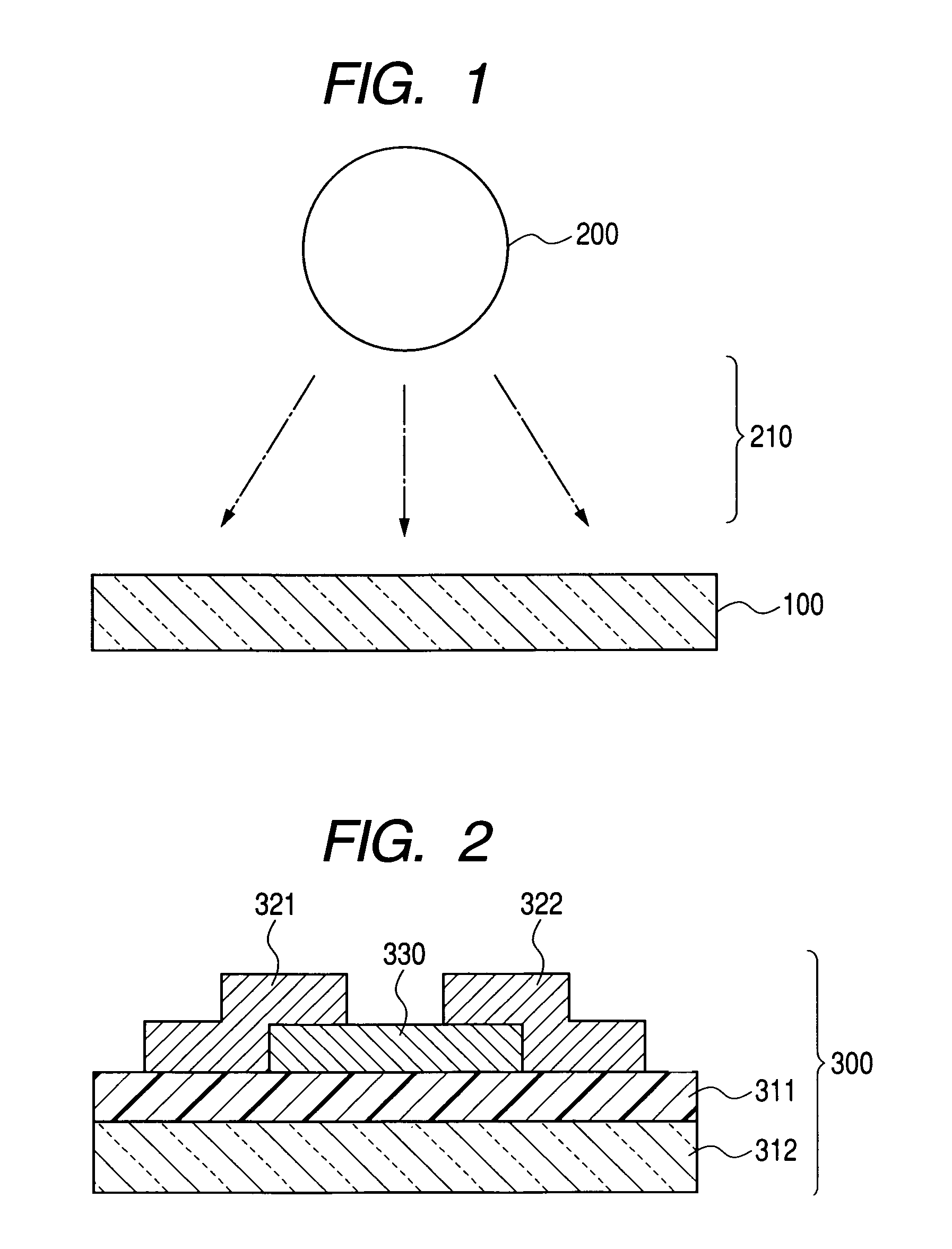
[0081]In the present example, a TFT was fabricated first, and a treatment according to the exemplary embodiment of the present invention was applied on the TFT, upon which condition possible influence of light irradiation on the TFT was considered.

(Fabrication of Amorphous IGZO film)

[0082]To begin with, an amorphous IGZO film being a semiconductor film was manufactured to evaluate physicality of the film.

[0083]As a film-forming substrate, a glass substrate (#1737, Corning Incorporated) having been degreased was prepared. As a target material, a polycrystalline sintered compact (with a diameter of 98 mm, a thickness of 5 mm, and an electrical conductance of 0.25 S·cm−1) with an InGaO3 (ZnO) composition was used. A total pressure inside a deposition chamber at film-forming was rendered 0.5 Pa by an oxygen-argon mixed gas containing 5 volume percent of oxygen. A distance between the target and the film-forming substrate was 75 mm. Film-forming was performed with a supply power of RF 20...

second example

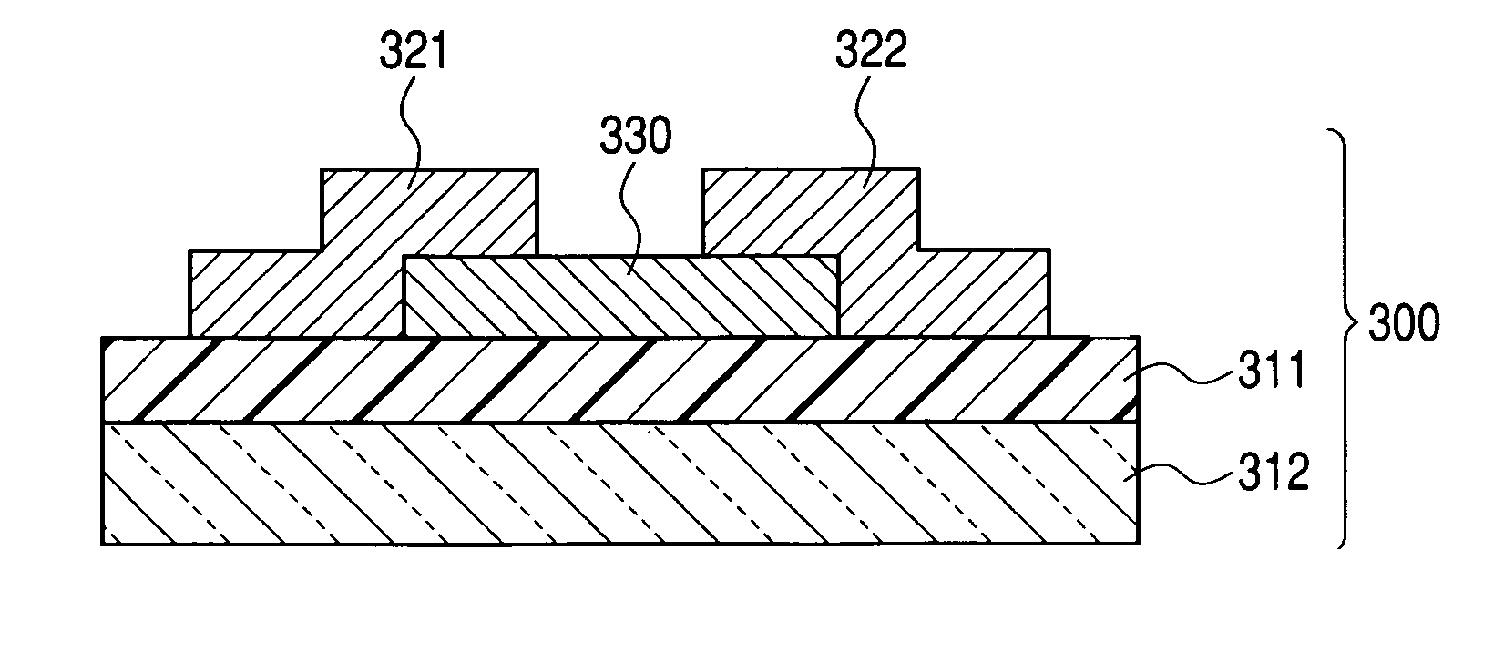
[0102]In the present example, a TFT was fabricated first, and a treatment according to the exemplary embodiment of the present invention was applied on the TFT, upon which condition evaluation was carried out.

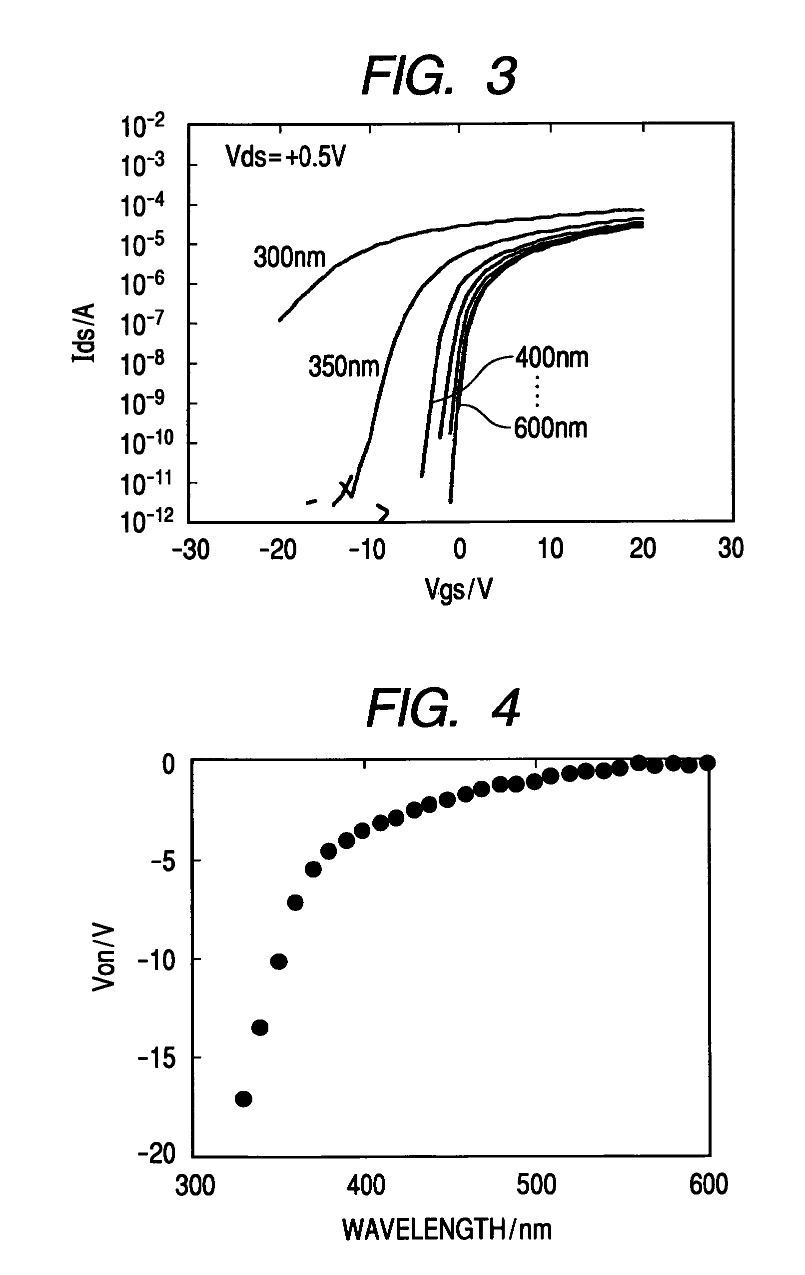
[0103]To begin with, an amorphous IGZO semiconductor was formed on an n+-silicon wafer with a thermally-oxidized silicon film (100 nm thick) to a thickness of 20 nm under the same conditions as in the case of the first example. An absorption edge wavelength of such amorphous IGZO semiconductor was estimated as follows. A phase difference and an amplitude ratio with respect to reflective polarized lights p and s were derived by ultraviolet-visible spectroscopic ellipsometry. Furthermore, fundamental (inter-band-edge) absorption and tail (subband) absorption were assumed as Tauc-Lorentz type absorption and Gaussian type absorption, respectively, on the basis of which a fitting analysis of the extinction coefficient and the refractive index was performed to meet the Kramers-Kronig...


PUM


Abstract

In a method of treating a semiconductor element which at least includes a semiconductor, a threshold voltage of the semiconductor element is changed by irradiating the semiconductor with light with a wavelength longer than an absorption edge wavelength of the semiconductor. The areal density of in-gap states in the semiconductor is 1013 cm−2eV−1 or less. The band gap may be 2 eV or greater. The semiconductor may include at least one selected from the group consisting of In, Ga, Zn and Sn. The semiconductor may be one selected from the group consisting of amorphous In—Ga—Zn—O (IGZO), amorphous In—Zn—O (IZO) and amorphous Zn—Sn—O (ZTO). The light irradiation may induce the threshold voltage shift in the semiconductor element, the shift being of the opposite sign to the threshold voltage shift caused by manufacturing process history, time-dependent change, electrical stress or thermal stress.

Description

TECHNICAL FIELD[0001]The present invention relates to a method of treating a semiconductor element. In particular, the present invention relates to a method of treating a semiconductor element using light irradiation.BACKGROUND ART[0002]Currently, with respect to a thin-film transistor (TFT), a wide variety of materials have been searched and considered for use as a channel layer, in an attempt to achieve high performance, low-temperature fabrication process, and low costs. From this perspective, possible materials for the channel layer may be, for example, amorphous silicon, polycrystal silicon, microcrystal silicon and organic semiconductor.[0003]In recent years, as a potent material to be used as such channel layer, an oxide semiconductor has been studied actively. For example, Barquinha et al., J. Non-Cryst. Sol., 352, 1756 (2006) and Yabuta et al., Appl. Phys. Lett., 89, 112123 (2006) disclose methods of fabricating a TFT using an amorphous In—Zn—O (IZO) thin film and an amorph...

Claims


Application Information

Patent Timeline
Patent Type & Authority Patents(United States)
IPC IPC(8): H01L21/331
CPCH01L29/78633H01L29/66969H01L29/7869H01L29/66742H01L29/78693
Inventor OFUJI, MASATOABE, KATSUMISHIMIZU, HISAEHAYASHI, RYOSANO, MASAFUMIKUMOMI, HIDEYATAKAI, YASUYOSHIKAWASAKI, TAKEHIKOKANEKO, NORIO
Owner CANON KK
Why Eureka
Try Eureka