Reflective mask blank for EUV lithography

a lithography and mask technology, applied in the field of reflection mask blanks, can solve the problems of accelerating microsizing of semiconductor devices, close to the resolution limit of conventional photolithography, etc., and achieve the effects of reducing contamination in the etching process, reducing the contamination of the etching process, and simplifying the etching process and the etching apparatus

Inactive Publication Date: 2012-03-20
ASAHI GLASS CO LTD
View PDF22 Cites 10 Cited by
  • Summary
  • Abstract
  • Description
  • Claims
  • Application Information

AI Technical Summary

Benefits of technology

[0039]In the EUV mask blank of the present invention, the low reflective layer contains no oxygen, and accordingly even in an etching process employing a chlorine type gas, a sufficiently high etching rate as compared with a conventional low reflective layer will be obtained. Accordingly, etching of the low reflective layer and the absorber layer is possible only by a chlorine type gas, whereby simplification of the etching process and the etching apparatus is expected and in addition, a reduction of contamination in the etching process is also expected. Further, in the present invention, as the etching rate for the low reflective layer is high as compared with a conventional low reflective layer, the resist can be made thinner than ever before, and as a result, it is expected that the finer patterning becomes possible.

Problems solved by technology

However, the conventional photolithography method has been close to the resolution limit, while microsizing of semiconductor devices has been accelerated.

Method used


Image

  • Reflective mask blank for EUV lithography
  • Reflective mask blank for EUV lithography

Examples


example 1

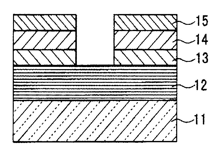
[0133]In this Example, an EUV mask blank 1 as shown in FIG. 1 was prepared.

[0134]As a substrate 11 for film deposition, a SiO2—TiO2 type glass substrate (shape: about 6 inch (about 152 mm) square, thickness: about 6.3 mm) was used. This glass substrate had a thermal expansion coefficient of 0.02×10⁻⁷ / ° C., a Young's modulus of 67 GPa, a Poisson's ratio of 0.17 and a specific rigidity of 3.07×10⁷ m2 / s2. This glass substrate was polished to form a smooth surface having a surface roughness (rms) of at most 0.15 nm with a flatness of at most 100 nm.

[0135]On the rear side of the substrate 11, a highly dielectric coating having a sheet resistance of 100 Ω / □ was applied by forming a Cr film having a thickness of 100 nm by using a magnetron sputtering method.

[0136]On a flat-plate-form usual electrostatic chuck, the substrate 11 (shape: 6 inch (152 mm) square, thickness: 6.3 mm) was fixed by means of the formed Cr film, and on the surface of the substrate 11, a Si film and a Mo film were alt...

example 2

[0194]In this Example, the same operation as in Example 1 was carried out except that as the absorber layer 14, a TaN film containing tantalum (Ta) and nitrogen (N) was formed by using a magnetron sputtering method.

[0195]The absorber layer 14 (TaN film) was formed by the following method. The film composition was examined in the same manner as in Example 1. The composition of the absorber layer 14 was Ta:N=57:43. The O content in the absorber layer was at most 0.05 at %.

Film Deposition Conditions for Absorber Layer 14 (TaN Film)

[0196]Target: Ta target

[0197]Sputtering gas: Ar and N2 (Ar: 86 vol %, N2: 14 vol %, gas pressure: 0.3 Pa)

[0198]Applied power: 150 W

[0199]Film deposition rate: 7.5 nm / min

[0200]Film thickness: 70 nm

[0201]Degree of vacuum before film deposition: 4×10⁻⁶ Pa

[0202]Then, on the absorber layer 14 (TaN film), a low reflective layer 15 (SiN film) was formed in the same manner as in Example 1 to obtain an EUV mask blank 1. With respect to the obtained EUV mask blank 1, t...

example 3

[0208]In this Example, an EUV mask blank 1 was obtained in the same manner as in Example 2 except that as the low reflective layer 15, a SiGeN film containing silicon (Si), germanium (Ge) and nitrogen (N) was formed by using a magnetron sputtering method. The low reflective layer 15 (SiGeN film) was formed by the following method.

Film Deposition Conditions for Low Reflective Layer 15 (SiGeN Film)

[0209]Target: SiGe target

[0210]Sputtering gas: mixed gas of Ar and N2 (Ar: 20 vol %, N2: 80 vol %, gas pressure: 0.3 Pa)

[0211]Applied power: 150 W

[0212]Film deposition rate: 2 nm / min

[0213]Film thickness: 10 nm

[0214]The film composition of the low reflective layer 15 (SiGeN) is examined in the same manner as in Example 1. The composition of the low reflective layer 15 is Si:Ge:N=29:5:66. The O content in the low reflective layer is at most 5 at %.

[0215]The crystalline state of the low reflective layer 15 (SiGeN) was examined in the same manner as in Example 1. The crystalline state of the low...


PUM

PropertyMeasurementUnit
wavelength rangeaaaaaaaaaa
surface roughnessaaaaaaaaaa
thicknessaaaaaaaaaa

Abstract

To provide a reflective mask blank for EUV lithography having a low reflective layer having a low reflectance in the wavelength region of EUV light and an inspection light for a mask pattern, particularly having low reflection properties in the entire wavelength region (190 to 260 nm) of an inspection light for a mask pattern, and having a high etching rate in chlorine type gas etching. A reflective mask blank for EUV lithography, comprising a substrate, and a reflective layer to reflect EUV light, an absorber layer to absorb EUV light and a low reflective layer to an inspection light (wavelength:190 nm to 260 nm) for a mask pattern, formed in this order over the substrate, wherein the low reflective layer contains silicon (Si) and nitrogen (N) in a total content of at least 95 at %, has a Si content of from 5 to 80 at %, and a N content of from 15 to 90 at %.

Description

CROSS-REFERENCE TO RELATED APPLICATIONS[0001]This application is a continuation application of and claims the benefit of priority from International Application No. PCT / JP2009 / 061048, filed Jun. 17, 2009, which claims the benefit of priority from Japanese Patent Application No. 2008-160344, filed Jun. 19, 2008. The contents of PCT / JP2009 / 061048 and JP2008-160344 are incorporated by reference herein in their entirety.TECHNICAL FIELD[0002]The present invention relates to a reflective mask blank (in this specification, hereinafter referred to as “EUV mask blank”) for EUV (Extreme Ultra Violet) lithography to be used for e.g. production of semiconductors.BACKGROUND ART[0003]In the semiconductor industry, a photolithography method using visible light or ultraviolet light has been employed as a technique for writing, on a Si substrate or the like, a fine pattern, which is required for forming an integrated circuit comprising such a fine pattern. However, the conventional photolithography ...

Claims


Application Information

Patent Timeline
Patent Type & Authority Patents(United States)
IPC IPC(8): G03F1/00B32B9/00G03F1/24G03F1/84
CPCB82Y10/00G03F1/84G03F1/24B82Y40/00Y10T428/31616G03F1/52H01L21/0275
Inventor HAYASHI, KAZUYUKI
Owner ASAHI GLASS CO LTD
Why Eureka
Try Eureka