
Interfacial capping layers for interconnects

a technology of interconnects and capping layers, which is applied in the direction of solid-state devices, basic electric elements, semiconductor devices, etc., can solve the problems of void formation, failure of devices, and electromigration failure of interconnects, and achieve the effects of increasing interconnect resistance, increasing interconnect resistance, and improving electromigration performance of interconnects

Active Publication Date: 2012-09-18
NOVELLUS SYSTEMS
View PDF59 Cites 13 Cited by
  • Summary
  • Abstract
  • Description
  • Claims
  • Application Information

AI Technical Summary

Benefits of technology

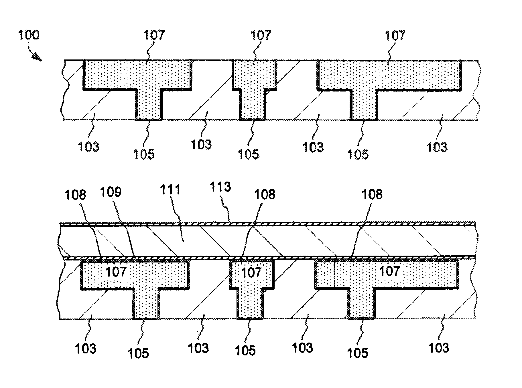
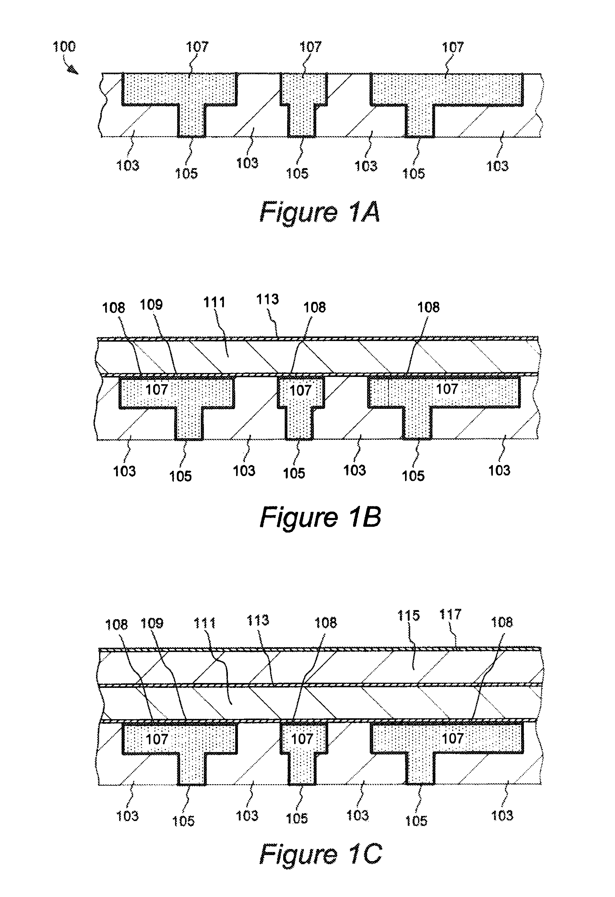
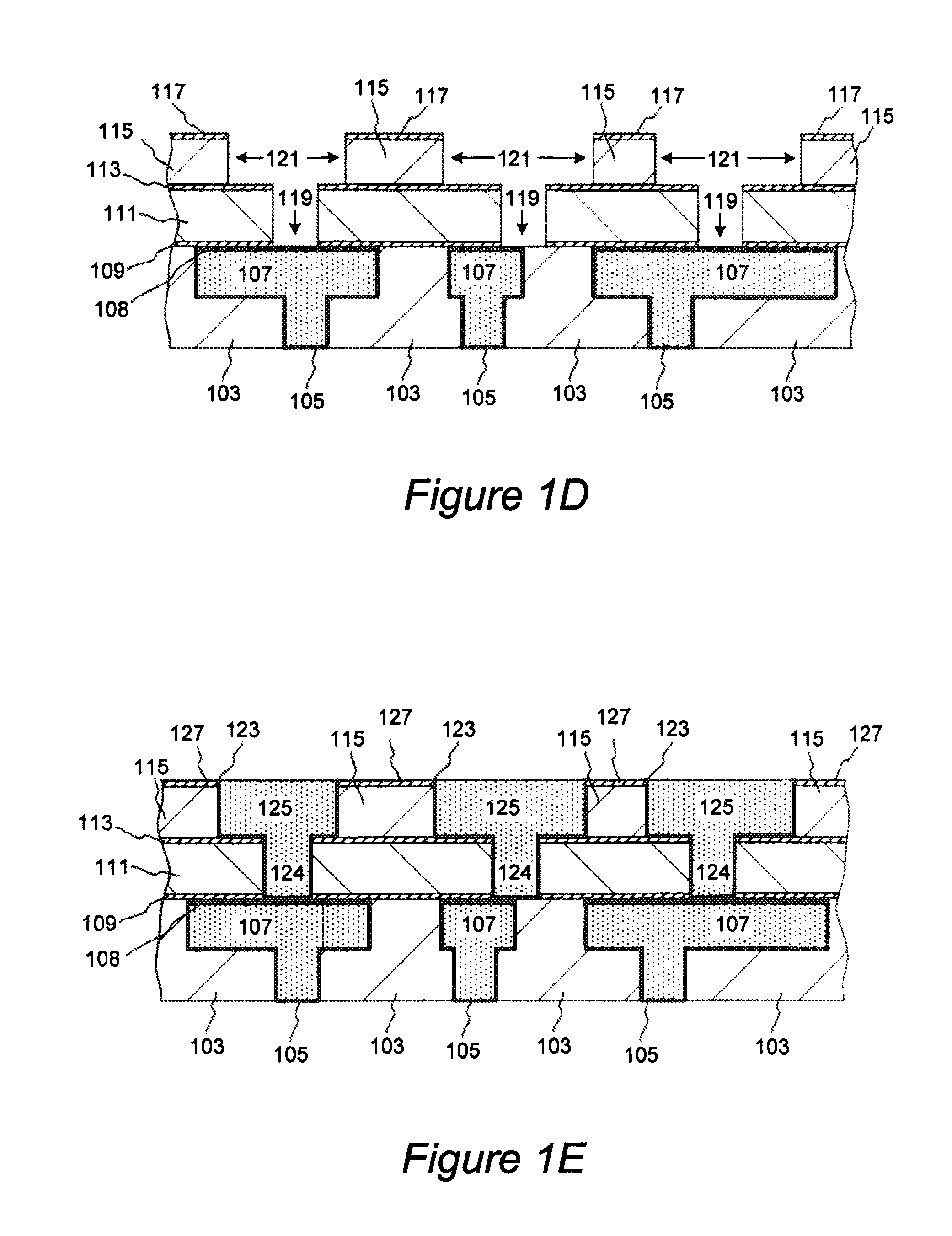
[0010]Adhesion layers residing at an interface between metal (e.g., copper) lines and dielectric diffusion barrier (or etch stop) layers that are capable of improving electromigration performance of interconnects are herein provided. Methods for forming such caps are also described. Advantageously, the described adhesion layers can be formed as very thin layers residing on the upper portion of a metal line at its interface with the dielectric diffusion barrier layer, without significantly increasing interconnect resistance. In some embodiments, no substantial diffusion of capping material into the metal line occurs, and the adhesion layer is cleanly segregated at the very top of the line, e.g., on or within the top portion of the line.
[0017]Notably, in many embodiments, the copper line resides in a layer of ultra low-k (ULK) dielectric having a dielectric constant of less than about 2.8. These materials are often mechanically weak and can be easily damaged. In some embodiments, pre-treatment of copper surface, and / or post-treatment of adhesion layer (e.g., nitridizing post-treatment) are performed such as to minimize damage to the exposed dielectric layer. In some cases, direct plasma treatment may be too damaging for porous and / or organic dielectric materials, and UV treatment, thermal treatment, or remote plasma treatments are preferred. Pre-clean, deposition of the precursor layer, and post-treatment may be performed in a CVD apparatus without a vacuum break, e.g., in the same process chamber. In some embodiments, it is preferable that the substrate remains in a reducing atmosphere throughout pre-clean, precursor layer deposition, and post-treatment processes.
[0024]The devices formed using these methods may have improved electromigration properties and also may exhibit greater adhesion at the metal / dielectric diffusion interface.

Problems solved by technology

One challenging problem encountered during IC fabrication is electromigration failure.
Electromigration occurs when high current densities experienced by an interconnect lead to migration of metal atoms with the current, and, consequently, lead to formation of voids within interconnects.
Ultimately, formation of voids may lead to failure of the device, known as electromigration failure.
As a consequence, the probability of electromigration failure increases with such device miniaturization.
While copper has a greater electromigration resistance than aluminum, even in copper interconnects, electromigration failure becomes a significant reliability problem at 45 nm technology node and at more advanced nodes.
Further, there is poor interfacial bonding energy and therefore poor adhesion between dielectric copper diffusion barrier layer (e.g., SiN, SiC, or SiCN) and copper line.
Poor adhesion has been attributed to the presence of surface copper oxide and / or weaker cohesive strength between dielectric diffusion barrier materials (e.g., SiN, SiC, or SiCN) and copper as compared to copper-metal interactions.

Method used


Image

  • Interfacial capping layers for interconnects
  • Interfacial capping layers for interconnects
  • Interfacial capping layers for interconnects

Examples


experimental examples

[0155]Certain disclosed embodiments were tested using 200 mm and 300 mm wafers. Aluminum atoms are detected on Cu surface having Cu—O surface bonds after exposing Cu to TMA at wafer temperature between 80 to 200° C. No plasma is used prior to and during TMA exposure. A direct plasma of NH3 is used for post-treatment after TMA exposure. Aluminum and oxygen atoms are detected at the interface of SiC / Cu layers for wafer treated with TMA prior to SiC deposition. There is no significant Al atom diffusion into SiC Cu bulk films after 400° C. 12 hr thermal annealing. In addition, there is no increase in Cu resistance upon TMA exposure and after 400° C. 12 hr thermal annealing. These results indicate that Al atoms on Cu surface are immobile. Film adhesion of SiC on Cu measured by 4-point bending technique shows significant improvement so that no delamination is observed at SiC / Cu interface.

[0156]In one example, the wafer comprising copper having surface oxide was preheated in N2 for 40 seco...


PUM

PropertyMeasurementUnit
Temperatureaaaaaaaaaa
Thicknessaaaaaaaaaa
Diffusion barrieraaaaaaaaaa

Abstract

Adhesive layers residing at an interface between metal lines and dielectric diffusion barrier (or etch stop) layers are used to improve electromigration performance of interconnects. Adhesion layers are formed by depositing a precursor layer of metal-containing material (e.g., material containing Al, Ti, Ca, Mg, etc.) over an exposed copper line, and converting the precursor layer to a passivated layer (e.g., nitridized layer). For example, a substrate containing exposed copper line having exposed Cu—O bonds is contacted with trimethylaluminum to form a precursor layer having Al—O bonds and Al—C bonds on copper surface. The precursor layer is then treated to remove residual organic substituents and to form Al—N, Al—H bonds or both. The treatment can include direct plasma treatment, remote plasma treatment, UV-treatment, and thermal treatment with a gas such as NH3, H2, N2, and mixtures thereof. A dielectric diffusion barrier layer is then deposited.

Description

CROSS-REFERENCE TO RELATED APPLICATIONS[0001]This application claims priority under 35 USC 119(e) from U.S. Provisional Patent Application No. 61 / 183,924 naming Yu et al. as inventors, titled “Interfacial Capping Layers for Interconnects,” filed Jun. 3, 2009, which is incorporated herein by reference in its entirety for all purposes.FIELD OF THE INVENTION[0002]The present invention pertains to methods of forming layers of material on a partially fabricated integrated circuit. Specifically, the invention pertains to methods for forming an adhesion layer on or within copper lines for improving adhesion of copper to dielectric diffusion barrier layers and therefore improving interconnect reliability.BACKGROUND[0003]Disclosed are methods of forming layers of material on a partially fabricated integrated circuit. Specifically, the disclosed methods form an adhesion layer on or within copper lines for improving electromigration properties of interconnects such as those used in Damascene s...

Claims


Application Information

Patent Timeline
IPC IPC(8): H01L21/4763H01L29/40
CPCH01L21/02074H01L21/76832H01L21/76888H01L21/76849H01L21/76883H01L21/76834
Inventor YU, JENGYIWU, HUI-JUNGDIXIT, GIRISHVAN SCHRAVENDIJK, BARTSUBRAMONIUM, PRAMODJIANG, GENGWEIANTONELLI, GEORGE ANDREWO'LOUGHLIN, JENNIFER
Owner NOVELLUS SYSTEMS
Learn More