Group III nitride semiconductor light-emitting device

a technology of nitride and semiconductor light-emitting devices, which is applied in the direction of semiconductor devices, basic electric elements, electrical equipment, etc., can solve the problems of complex and redundant process for forming rgb-type white leds, inability to achieve light-emitting devices with high luminous intensity, and inability to achieve high luminous intensity. , to achieve the effect of high and stable color rendering properties of white light emission

Inactive Publication Date: 2013-03-05
RESONAC HOLDINGS CORPORATION
View PDF40 Cites 23 Cited by
  • Summary
  • Abstract
  • Description
  • Claims
  • Application Information

AI Technical Summary

Benefits of technology

[0022]According to the first aspect of the invention, the light-emitting layer has the multiple quantum well structure comprising the barrier layers and the well layers. According to this constitution, a white light-emitting device can be easily formed with a simple structure, and since the installation area is substantially the same as the plane area of the light-emitting layer, the luminous intensity can be enhanced. Although only one light-emitting layer is provided, by virtue of the use of the light-emitting layer having the multiple quantum well structure capable of providing multiwavelength emission, only the single light-emitting layer may be provided with p-type and n-type electrodes. As compared with the case of the conventional RGB-type white LED, a region of the light-emitting layer that should be scraped and removed can be significantly reduced, and the luminous efficiency can be improved.
[0028]According to the third aspect of the invention, the light-emitting layer having the multiple quantum well structure is constituted by using a plurality of well layers having different atomic concentrations of the acceptor impurities added thereto and providing a plurality of emissions with different wavelengths. Consequently, the single light-emitting layer independently providing multiwavelength emission can be obtained, and it is possible to provide a white LED with more excellent color rendering properties than, for example, the so-called complementary color type white LED which provides white light by mixing two lights which are in a relationship of complementary colors and have different wavelengths.

Problems solved by technology

That is, since the plane area occupied by the light-emitting layers providing light emission is extremely smaller than the plane area required for installation of the lamps, it is disadvantageous in obtaining a light-emitting device with high luminous intensity (lumen / area).
Thus, it is never advantageous in obtaining a light-emitting element with higher luminous intensity.
Thus, the process for forming the RGB-type white LED is complex and redundant.
Since the electrodes need to be provided in the clad layer of the conductivity type corresponding to each of the electrodes and the like, the light-emitting layer is scraped and removed, leading to deterioration of the luminous intensity of each emission.
Thus, when a white LED of the complementary color type is formed, a complex and redundant process is required like the case of the RGB-type white LED.
173-174), the total plane area of the light-emitting layer emitting blue or yellow light is smaller than the plane area required for arranging the LED, and therefore, it is not necessarily advantageous to obtain a light-emitting device with high luminous intensity.
In addition, in the complementary color type white LED, there is a problem that the color tone of resulting white light is slightly changed, depending on the wavelength of light of two colors in a complementary relationship that are mixed with each other to obtain the white light.
In the complementary color type white LED, colors of at most two lights with different wavelengths are usually mixed, and therefore, in any case, it is technically difficult to stably obtain a white LED exhibiting high and stable color rendering properties.
In the fluorescent-type white LED, in order to stably obtain white light with a fixed color tone by excitation of the phosphor, the wavelength of the light emitted from the light-emitting layer, which acts as an excitation light, should be kept constant with good reproducibility, and thus it is technically difficult.

Method used


Image

  • Group III nitride semiconductor light-emitting device
  • Group III nitride semiconductor light-emitting device
  • Group III nitride semiconductor light-emitting device

Examples


first embodiment

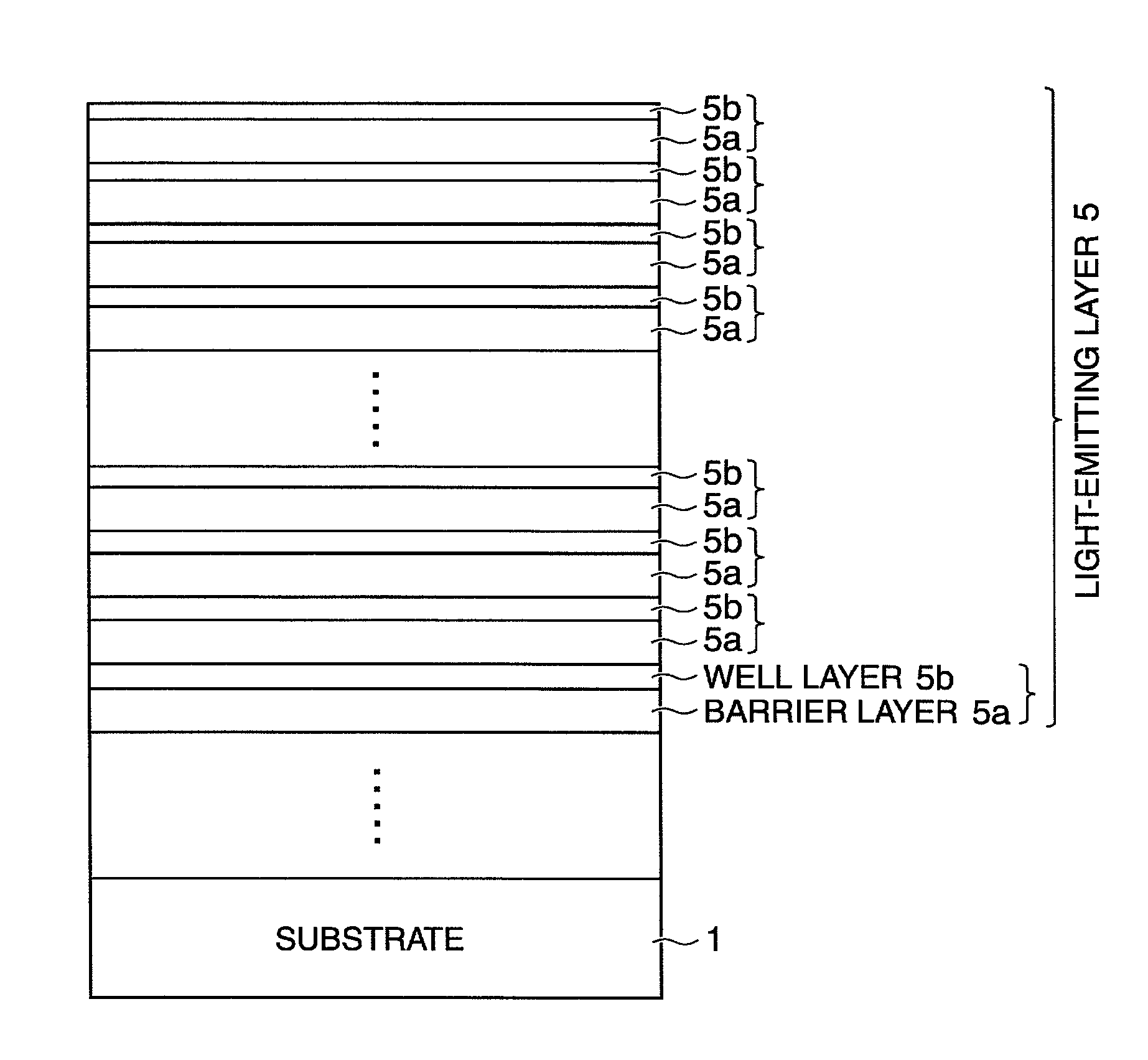
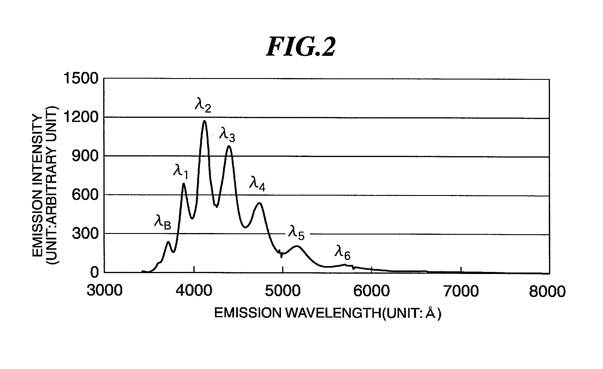
[0064]FIG. 3 is a schematic cross-sectional view showing a structure of a Group III nitride semiconductor light-emitting device comprising a light-emitting layer having the multiple quantum well structure of a first embodiment. FIG. 4 shows a photoluminescence spectrum radiated from the light-emitting layer having the multiple quantum well structure. In FIG. 4, the horizontal axis represents emission wavelength (unit: Å), and the vertical axis represents emission intensity (unit: arbitrary unit).

[0065]In the formation of a structure for use in production of a Group III nitride semiconductor light-emitting device 10, a {111} silicon single crystal (silicon) was used as a substrate 101.

[0066]The surface of the substrate 101 was cleaned with an inorganic acid, and thereafter the substrate 101 was conveyed into a growth chamber of a molecular beam epitaxy (MBE) growth system. The growth chamber was then evacuated to ultra-high vacuum. Thereafter, the temperature of the substrate 101 was...

second embodiment

[0076]FIG. 5 is a cross-sectional view schematically showing a constitution of a light-emitting layer having the multiple quantum well structure of a Group III nitride semiconductor light-emitting device (LED) of the second embodiment.

[0077]A light-emitting layer 205 having the multiple quantum well structure shown in FIG. 5 was formed, by nitrogen plasma MBE, on a stacked structure comprising the AlN layer, the AlGaN mixed crystal layer, and the n-type GaN layer (204 in FIG. 5) described in the first embodiment and provided on the Si substrate. The light-emitting layer 205 was formed as follows.

[0078]In the formation of the light-emitting layer 205 having the multiple quantum well structure, an n-type GaN barrier layer 205a having a thickness of 16 nm is first provided on the n-type GaN layer 204 by nitrogen plasma MBE. Then, an Mg doped Ga0.80In0.20N well layer as an n-type well layer 205b constituting the multiple quantum well structure was provided so that the n-type well layer ...

third embodiment

[0084]FIG. 7 is a schematic cross-sectional view showing a structure of a Group III nitride semiconductor light-emitting device comprising a light-emitting layer having the multiple quantum well structure of a third embodiment. FIG. 8 is a photoluminescence spectrum in a stacked structure for use in a Group III nitride semiconductor light-emitting device (LED) comprising the light-emitting layer having the multiple quantum well structure of the third embodiment.

[0085]By virtue of nitrogen plasma BME, the light-emitting layer having the multiple quantum well structure was formed on the stacked structure that comprises the AlN layer and the AlGaN mixed crystal layer (303 in FIG. 7) described in the first and second embodiments and provided on an Si substrate. The light-emitting layer is formed as follows.

[0086]In the formation of the light-emitting layer having the multiple quantum well structure, an n-type GaN barrier layer 305a with a thickness of 10 nm was first provided on the AlG...


PUM


Abstract

A Group III nitride semiconductor light-emitting device comprises a substrate (1) and a light-emitting layer (5) having the multiple quantum well structure that comprises barrier layers (5a) and well layers (5b) formed of a gallium-containing Group III nitride semiconductor material provided on the substrate. Each of the well layers constituting the multiple quantum well structure is made of a Group III nitride semiconductor layer to which acceptor impurities are added, and which has thicknesses different from one another and the same conductivity type as that of the barrier layer. The present invention can provide a Group III nitride semiconductor white light-emitting device which can enhance luminous intensity, can obtain high color rendering properties has a simple structure that can be easily formed without fine adjustment of a composition of a phosphor.

Description

CROSS REFERENCE TO RELATED APPLICATIONS[0001]This application is a National Stage of International Application No. PCT / JP2008 / 065914 filed Aug. 28, 2008, claiming priority based on Japanese Patent Application No. 2007-251167 filed Sept. 27, 2007, the contents of all of which are incorporated herein by reference in their entirety.TECHNICAL FIELD[0002]The present invention relates to a Group III nitride semiconductor light-emitting device comprising a substrate and a light-emitting layer having the multiple quantum well structure that comprises barrier layers and well layers formed of a gallium-containing Group III nitride semiconductor material provided on the surface of the substrate.BACKGROUND ART[0003]A Group III nitride semiconductor material such as gallium indium nitride (GaInN) has been conventionally used for a light-emitting layer of a short-wavelength light-emitting diode (abbr.: LED) of, for example, white or blue or a laser diode (abbr.: LD) (see, for example, JP-B No. 55...

Claims


Application Information

Patent Timeline
Patent Type & Authority Patents(United States)
IPC IPC(8): H01L33/04H01L33/32H01L33/06H01L33/20
CPCH01L33/06H01L33/08H01L33/32
Inventor KIKUCHI, TOMOUDAGAWA, TAKASHI
Owner RESONAC HOLDINGS CORPORATION
Why Eureka
Try Eureka