Logic circuit and semiconductor device

a logic circuit and semiconductor technology, applied in logic circuit coupling/interface arrangement, semiconductor/solid-state device testing/measurement, pulse technique, etc., can solve the problems of low on-off ratio of thin film transistors, unstable operation of circuits including thin film transistors with low on-off ratios, etc., to reduce hydrogen concentration, suppress the leakage of electric charge stored in capacitors, and reduce the effect of hydrogen concentration

Active Publication Date: 2013-03-19
SEMICON ENERGY LAB CO LTD
View PDF223 Cites 44 Cited by
  • Summary
  • Abstract
  • Description
  • Claims
  • Application Information

AI Technical Summary

Benefits of technology

[0010]The on-off ratio is a measure of characteristics of a switch. Operation of a circuit including a thin film transistor with a low on-off ratio becomes unstable. Further, current flows excessively due to large off-state current; thus, power consumption is increased.
[0011]In view of the foregoing problems, an object of an embodiment of the present invention is to suppress a malfunction of a logic circuit including a thin film transistor formed using an oxide semiconductor.
[0012]Further, an object of an embodiment of the present invention is to reduce power consumption of a logic circuit including a thin film transistor formed using an oxide semiconductor.
[0020]In accordance with an embodiment of the present invention, a logic circuit includes a thin film transistor having a channel formation region formed using an oxide semiconductor; and a capacitor having terminals one of which is brought into a floating state by turning off the thin film transistor. The oxide semiconductor is an oxide semiconductor with reduced hydrogen concentration. Specifically, the hydrogen concentration of the oxide semiconductor is 5×10¹⁹ (atoms / cm3) or less, and when there is no electric field, the oxide semiconductor serves as an insulator or a semiconductor which is close to an insulator (the semiconductor which is close to an insulator is substantially an insulator). Therefore, off-state current of the thin film transistor can be reduced. Thus, the leakage of electric charge stored in the capacitor, through the thin film transistor, can be suppressed. Thus, a malfunction of the logic circuit can be prevented. Further, a period where the one terminal of the capacitor is in a floating state can be made long. In other words, the number of times of data rewriting to the capacitor (also referred to as refreshing) can be reduced.
[0021]Furthermore, the excessive amount of current which flows in the logic circuit can be reduced through the reduction of off-state current of the thin film transistor. Thus, power consumption of the logic circuit can be reduced.

Problems solved by technology

However, a difference from the stoichiometric composition in the oxide semiconductor arises in a thin film formation process.
Such a low on-off ratio of the thin film transistor is due to large off-state current.
Operation of a circuit including a thin film transistor with a low on-off ratio becomes unstable.
Further, current flows excessively due to large off-state current; thus, power consumption is increased.

Method used


Image

  • Logic circuit and semiconductor device
  • Logic circuit and semiconductor device
  • Logic circuit and semiconductor device

Examples


embodiment 1

(Embodiment 1)

[0056]In this embodiment, examples of logic circuits are described. Specifically, examples of inverters each including a thin film transistor having a channel formation region which is formed using an oxide semiconductor are described with reference to FIGS. 1A to 1D and FIGS. 2A to 2D.

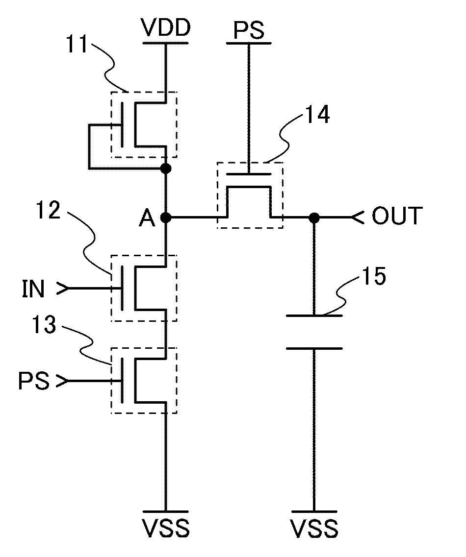
[0057]FIG. 1A is a circuit diagram illustrating an example of an inverter of this embodiment. The inverter illustrated in FIG. 1A includes thin film transistors 11 to 14 and a capacitor 15. Here, the thin film transistor 11 is a depletion type transistor and the thin film transistors 12 to 14 are enhancement type transistors. Note that in this specification, an n-channel transistor whose threshold voltage is positive is referred to as an enhancement type transistor, and an n-channel transistor whose threshold voltage is negative is referred to as a depletion type transistor.

[0058]A first terminal of the thin film transistor 11 is electrically connected to a wiring for supplying a high po...

embodiment 2

(Embodiment 2)

[0090]In this embodiment, examples of logic circuits are described. Specifically, examples of shift registers each including the inverter in Embodiment 1 are described with reference to FIGS. 3A and 3B and FIGS. 4A and 4B.

[0091]A shift register of this embodiment includes a plurality of pulse output circuits; a wiring for supplying a first clock signal (CK1), which is electrically connected to odd-numbered pulse output circuits of the plurality of pulse output circuits (hereinafter, such a wiring is also referred to as a first clock signal line); and a wiring for supplying a second clock signal (CK2), which is electrically connected to even-numbered pulse output circuits of the plurality of pulse output circuits (hereinafter, such a wiring is also referred to as a second clock signal line). Further, an input terminal of each pulse output circuit is electrically connected to a wiring for supplying a start pulse signal (SP) (hereinafter, such a wiring is also referred to...

embodiment 3

(Embodiment 3)

[0146]In this embodiment, an example of thin film transistors included in the logic circuit in Embodiment 1 or Embodiment 2 is described.

[0147]One embodiment of a thin film transistor and a manufacturing method of the thin film transistor of this embodiment is described with reference to FIGS. 5A and 5B and FIGS. 6A to 6E.

[0148]FIGS. 5A and 5B illustrate an example of a planar structure and a cross-sectional structure of a thin film transistor. A thin film transistor 410 illustrated in FIGS. 5A and 5B is one of top gate thin film transistors.

[0149]FIG. 5A is a plan view of the thin film transistor 410 having a top-gate structure and FIG. 5B is a cross-sectional view taken along a line C1-C2 in FIG. 5A.

[0150]The thin film transistor 410 includes, over a substrate 400 having an insulating surface, an insulating layer 407, an oxide semiconductor layer 412, a source or drain electrode layer 415a, a source or drain electrode layer 415b, a gate insulating layer 402, and a ga...


PUM


Abstract

A logic circuit includes a thin film transistor having a channel formation region formed using an oxide semiconductor, and a capacitor having terminals one of which is brought into a floating state by turning off the thin film transistor. The oxide semiconductor has a hydrogen concentration of 5×10¹⁹ (atoms / cm3) or less and thus substantially serves as an insulator in a state where an electric field is not generated. Therefore, off-state current of a thin film transistor can be reduced, leading to suppressing the leakage of electric charge stored in a capacitor, through the thin film transistor. Accordingly, a malfunction of the logic circuit can be prevented. Further, the excessive amount of current which flows in the logic circuit can be reduced through the reduction of off-state current of the thin film transistor, resulting in low power consumption of the logic circuit.

Description

TECHNICAL FIELD[0001]One aspect of the present invention relates to a logic circuit including a field-effect transistor formed using an oxide semiconductor. Further, one aspect of the present invention relates to a semiconductor device including the logic circuit.[0002]Note that a semiconductor device in this specification indicates all the devices that can operate by using semiconductor characteristics, and electro-optical devices, semiconductor circuits, and electronic appliances are all included in the category of the semiconductor devices.BACKGROUND ART[0003]Much attention has been paid to a technology of forming a thin film transistor (TFT), by using a thin semiconductor film that is formed over a substrate having an insulating surface. A thin film transistor is used for a display device typified by a liquid crystal television. A silicon-based semiconductor material is known as a material for a thin semiconductor film applicable to a thin film transistor. Other than a silicon-b...

Claims


Application Information

Patent Timeline
Patent Type & Authority Patents(United States)
IPC IPC(8): H01L25/00H03K19/094H03B1/00
CPCH01L27/1225H01L29/7869H01L29/78696H01L22/34H01L2924/0002H01L2924/00H01L29/06H01L27/0207
Inventor YAMAZAKI, SHUNPEIKOYAMA, JUNTSUBUKU, MASASHINODA, KOSEI
Owner SEMICON ENERGY LAB CO LTD
Why Eureka
Try Eureka