Switching circuit and imaging apparatus utilizing the same

a technology of switching circuit and imaging apparatus, which is applied in the direction of television system, pulse technique, instruments, etc., can solve the problems of delay in the turn-off of pch-mosfet, incomplete horizontal transfer, and lowering of horizontal resolving power, so as to reduce heat liberation and temperature rise, reduce power loss, and enhance the effect of temperature variation

Inactive Publication Date: 2013-03-26
KOKUSA ELECTRIC CO LTD
View PDF6 Cites 0 Cited by
  • Summary
  • Abstract
  • Description
  • Claims
  • Application Information

AI Technical Summary

Benefits of technology

[0015]Namely, an object of the present invention is to solve the above-described problems by preventing an attenuation of the amplitude of the load capacity, and improving the rectangular-wave characteristics while reducing a feedthrough current at which the Nch-MOSFET and the Pch-MOSFET are mutually brought into the simultaneous conduction.
[0018]Namely, according to the present invention, there is provided the following switching circuit: In the inversion switching circuit, a high-frequency current, i.e., the main component of a feedthrough current, is limited by lowering the electrodes-in-series impedance of the semiconductor devices at a load-driving-pulse frequency, and heightening the electrodes-in-series impedance of the semiconductor devices at a feedthrough-current frequency, or by lowering the electrodes-in-series impedance of the semiconductor devices in a conduction-start (i.e., turn-on) direction, and heightening the electrodes-in-series impedance of the semiconductor devices in a conduction-termination (i.e., turn-off) direction.
[0021]Also, according to the present invention, the high-frequency current is reduced, which is the main component of the feedthrough current at which the Pch-MOSFET and the Nch-MOSFET are mutually brought into the simultaneous conduction. As a result, the power loss is decreased to decrease the heat liberation and temperature rise by the amount corresponding to the power loss. Accordingly, the sensitivity of the EM-CCD, which varies by the amount of 1.8 times as a result of a 11-° C. temperature variation, is enhanced even further.
[0022]Furthermore, a high impedance unit is inserted in parallel to the conduction-termination (i.e., turn-off) direction diode which is inserted into the gate electrodes of the Pch-MOSFET and the Nch-MOSFET in series therewith. This insertion short-circuits a conduction-start (i.e., turn-on) direction diode which is inserted into the gate electrodes of the Pch-MOSFET and the Nch-MOSFET in series therewith, eliminates the forward-direction drop voltage of the conduction-start (i.e., turn-on) direction diode, sufficiently ensures the gate-source voltages of the Pch-MOSFET and the Nch-MOSFET at the time of the conduction, lowers the ON resistances of the Pch-MOSFET and the Nch-MOSFET at the time of the conduction, and improves the rectangular-wave characteristics of the CMG voltage, thereby enhancing the sensitivity of the EM-CCD even further. The improvement of the rectangular-wave characteristics of the CMG voltage makes it highly unlikely that there will occur the lowering in the horizontal resolving power at the high electron-multiplying time when the CMG voltage amplitude is large, and that there will occur the blooming, i.e., the phenomenon that charge carriers, which leak out to a vertical transfer path due to an excessive light amount, overflow one after another from an accumulation-unit transfer path to a horizontal transfer path.

Problems solved by technology

Consequently, unlike other electrode drivings for the CCD imaging device, it is difficult to utilize the general-purpose integrated circuit whose withstand voltage is equal to about 18 V. In view of this situation, the following technique is commonly used: A pulse waveform is supplied to the CMG for performing the electron multiplication of the EM-CCD via the drain of a complementary enhancement-type metal-oxide-semiconductor field-effect transistor (: MOSFET) whose power-supply voltage is variable.
It is estimated that the lowering in the horizontal resolving power occurs because, at the high electron-multiplying time when the CMG voltage amplitude is large, rectangular-wave characteristics of the CMG deteriorate and thus the horizontal transfer becomes incomplete.
As a result, the Pch-MOSFET is delayed in its turn-off.
Also, since the value of Qg1 is large, Vcmg becomes unbalanced.
Consequently, the above-described conventional technologies, where the conduction time and the non-conduction time are made substantially equal to each other, is inapplicable to the CMG driving.
On account of this, there occurs a simultaneous conduction time during which the Nch-MOSFET and the Pch-MOSFET are simultaneously brought into the conduction, which gives rise to the consumption of ineffective power.
Accordingly, it is expected that the heat liberation amount will increase by the amount equivalent to a significant loss due to the ineffective power, and that the temperature will rise thereby to lower the sensitivity of the EM-CCD.
Moreover, the blooming in the horizontal transfer becomes deteriorated.

Method used


Image

  • Switching circuit and imaging apparatus utilizing the same
  • Switching circuit and imaging apparatus utilizing the same
  • Switching circuit and imaging apparatus utilizing the same

Examples


Embodiment Construction

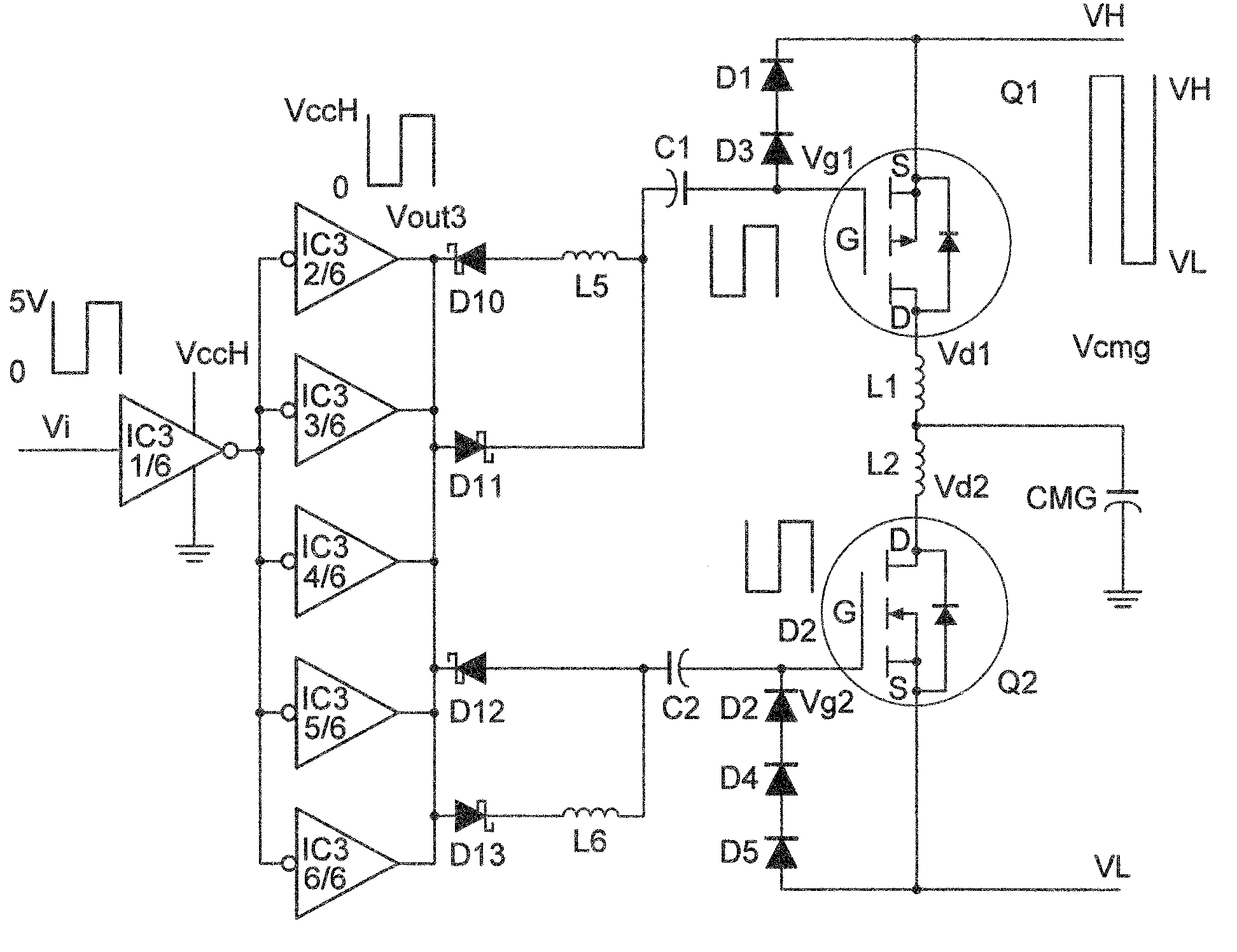
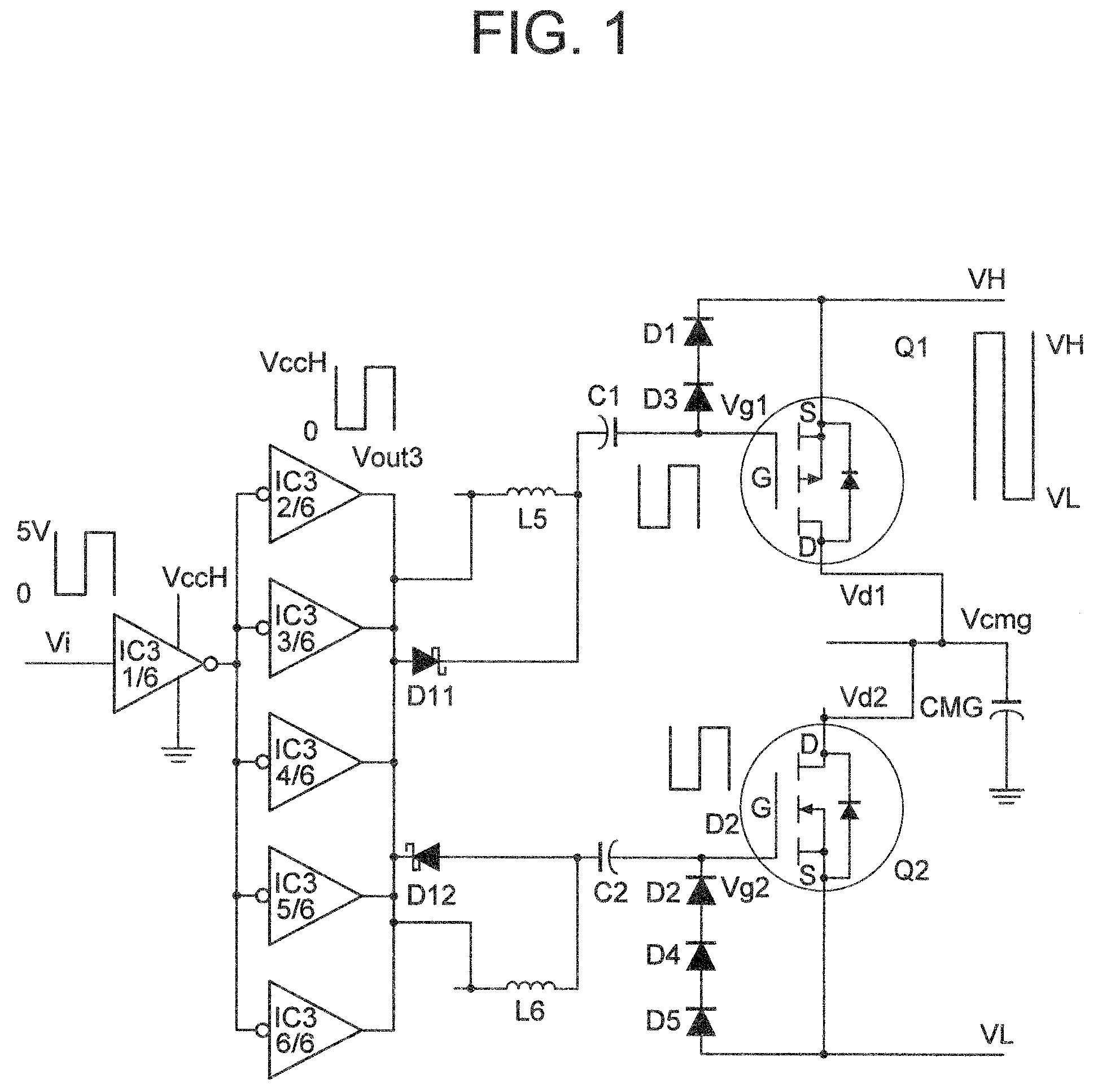
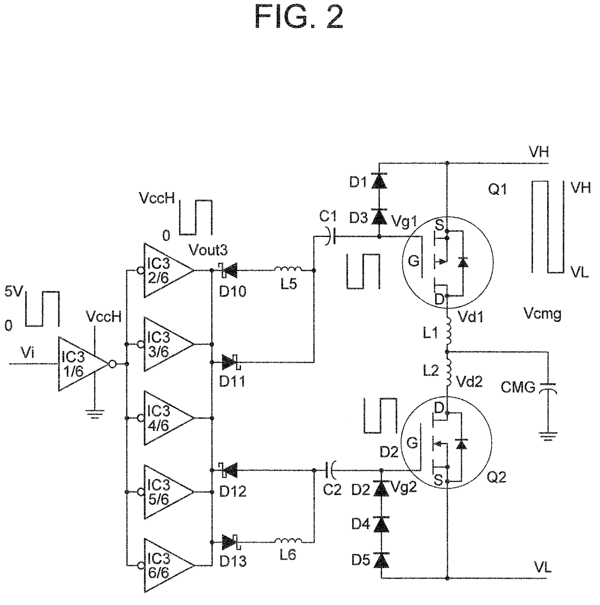
[0033]Hereinafter, referring to a block diagram in FIG. 9, the explanation will be given below concerning an imaging apparatus where a switching circuit according to an embodiment of the present invention is used for driving the charge multiplication gate (CMG) of the electron-multiplying charge-coupled-device (EM-CCD) imaging device. Moreover, the explanation will be given below regarding the switching circuit according to the embodiment of the present invention, referring to block diagrams illustrated in FIG. 1, FIG. 2, and FIG. 3, and waveform schematic diagrams illustrated in FIG. 4, FIG. 5, and FIG. 6.

[0034]FIG. 9 is the block diagram for illustrating the configuration of the imaging apparatus using the EM-CCD imaging device. In FIG. 9, the reference numeral 1 denotes the imaging apparatus, and 2 denotes a lens. Inside the imaging apparatus, 3 denotes the EM-CCD, 4 denotes a FEP (Front End Processor), 5 denotes a video-signal processing unit, 6 denotes a CPU, 7 denotes a timing...


PUM

PropertyMeasurementUnit
power-supply voltageaaaaaaaaaa
voltage amplitudeaaaaaaaaaa

Abstract

In a complementary-MOSFET driving circuit for driving the charge multiplication gate of an EM-CCD, a ferrite bead is connected to a conduction-termination direction diode in parallel thereto, the conduction-termination direction diode being inserted into the gate electrodes of complementary MOSFETs in series therewith, the impedance of the ferrite bead at a switching frequency being lower than one-half of the gate-electrode impedance of the MOSFETs, a time during which the MOSFETs are brought into simultaneous conduction being shorter than ¼th of the switching period, the impedance of the ferrite bead at a frequency equivalent to ¼th of the switching period being higher than 2 times the gate-electrode impedance of the MOSFETs, a ferrite bead being connected to the drain electrodes of the complementary MOSFETs in series therewith, the impedance of the ferrite bead at the switching frequency being lower than one-half of the impedance of a capacitive load at the switching frequency, and the impedance of the ferrite bead, at a frequency equivalent to ¼th of the switching period being higher than 2 times the impedance of the capacitive load.

Description

INCORPORATION BY REFERENCE[0001]The present application claims priority from Japanese application JP2008-143158 filed on May 30, 2008, the content of which is hereby incorporated by reference into this application.BACKGROUND OF THE INVENTION[0002]The present invention relates to a switching circuit of capacitive load. More particularly, it relates to an improvement in the driving circuit for charge multiplication gate of an electron-multiplying charge-coupled-device imaging device.[0003]As the charge-multiplication-gate driving circuit of the charge-coupled-device (which, hereinafter, will be abbreviated as “CCD”) imaging device as well, the driving logic integrated circuit for the CCD imaging device is available if voltage amplitude of the driving-target CCD imaging device is smaller than 5 V. Also, the general-purpose CMOS logic integrated circuit is available if the voltage amplitude is smaller than 6 V (reference should be made to the SONY-fabricated ICX422AL 11-mm diagonal (2 / 3...

Claims


Application Information

Patent Timeline
Patent Type & Authority Patents(United States)
IPC IPC(8): G01N30/86H03K17/16H03K17/687H04N5/335H04N5/372H04N5/376
CPCH03K17/6877H03K2217/0036
Inventor NAKAMURA, KAZUHIKOMUTO, YUTAKAKOGO, KIYOTAKA
Owner KOKUSA ELECTRIC CO LTD
Why Eureka
Try Eureka