Methods of preparing semiconductive compositions and devices

a technology of arylene diimide and composition, applied in the field of preparing thin films of arylene diimide compounds, can solve the problems of requiring relatively costly processes, limited application of amorphous silicon to low-speed devices, etc., and achieves the effects of convenient preparation, convenient and convenient preparation, and readily available materials

Inactive Publication Date: 2013-09-10
EASTMAN KODAK CO
View PDF20 Cites 2 Cited by
  • Summary
  • Abstract
  • Description
  • Claims
  • Application Information

AI Technical Summary

Benefits of technology

[0066]The present invention provides a way to make thin-film transistor devices and other semiconducting articles that address two challenges: (i) obtaining semiconducting diimides in solid thin films from solvent-soluble precursors, and (ii) using such precursors to generate diimides in solid state for achieving n-type transport in thin film transistors. Accordingly, the present invention can be used to provide devices and articles containing semiconducting arylene diimides that are obtained via solid state thermal dehydration imidization reaction of organic-soluble precursor amic acids or amic esters of diimide compounds. The amic acid and amic ester precursors can be easily prepared in environmentally friendly solvents like methanol, ethanol, water, or mixtures thereof. The arylene diimides obtained by solid state thermal conversion of amic acids and amic esters can be readily used to fabricate OTFT devices.
[0067]The advantages of these invention are achieved by preparing thin films of semiconducting arylene diimides by solid state thermal dehydration imidization reaction of amic acid or amic ester precursor or mixture thereof. Such thin films can be readily and conveniently prepared by applying a suitable solution of the amic acid or amic ester precursor onto a substrate and thereafter removing the solvent(s). The desired semiconducting arylene diimide can then be obtained by a thermal dehydration imidization reaction. The low temperature processing combined with readily available materials and ease of deposition of thin films over large areas due to solubility of the amic acids and amic esters provide an inexpensive approach to the fabrication of thin film transistor devices according to the present invention. Furthermore, materials and processes used in the present invention afford easy solution processability to arylene diimide based n-type semiconducting materials, without significant structural modification, which themselves may not be very organic solvent soluble.
[0069]In accordance with the present invention, the organic semiconductor layer generated by solid state conversion of thin films of soluble amic acid or amic ester precursors to the arylene diimide compounds, when used in the form of an n-channel layer, can exhibit high performance under inert conditions as well as in air without the need for special chemical underlayers.

Problems solved by technology

Application of amorphous silicon is limited to low speed devices, however, since its maximum mobility (0.5-1.0 cm2 / V·sec) is about a thousand times smaller than that of crystalline silicon.
The deposition of amorphous silicon, during the manufacture of transistors, requires relatively costly processes, such as plasma enhanced chemical vapor deposition and high temperatures (about 360° C.) to achieve the electrical characteristics sufficient for display applications.
Such high processing temperatures disallow the use of substrates, for deposition, made of certain plastics that might otherwise be desirable for use in applications such as flexible displays.
One such naphthalene-based n-channel semiconductor material, tetracyanonaphthoquino-dimethane (TCNNQD), is capable of operation in air, but the material has displayed a low on / off ratio and is also difficult to prepare and purify.
In crystalline organic films defects, like grain boundaries and disorder inside the grains, are limiting factors for the mobility and the diffusion length of the charge carriers.
However, this publication fails to suggest any comparative advantage of using cycloalkyl groups on the imide nitrogens.
Furthermore, the highest mobilities reported in this reference were 0.2 cm2 / V·sec and it fails to show experimental data with respect to naphthalene compounds and require that their core be dicyano disubstituted.
As is clear from the foregoing discussion, the development of new semiconducting materials, both p-type and n-type, continues to be an enormous topic of interest and unpredictable as to the semiconductive properties of various compounds.
However, the poor solubility of this material limits its practical application potential.
However, these authors do not disclose amic acids and amic esters of naphthalene tetracrboxylic acids or anhydrides.
However, these authors do not disclose the preparation of amic acid or amic ester from naphthalene dianhydride.

Method used


Image

  • Methods of preparing semiconductive compositions and devices
  • Methods of preparing semiconductive compositions and devices
  • Methods of preparing semiconductive compositions and devices

Examples


invention example 1

Preparation of 1,5-Naphthalenedicarboxylic acid-4,8-bis[(dodecylamino)-carbonyl]

[0258]

[0259]To a stirred dispersion of freshly sublimed 1,4,5,8 naphthalene tetracarboxylic acid dianhydride (46 mg) in dimethylacetamide (4 ml), a solution of dodecylamine (67 mg) in dimethylacetamide (1 ml) was added dropwise to obtain a clear pale yellow solution. Solvent was removed under reduced pressure to obtain an oily solid. 1H and 13C NMR spectra of the product were consistent with assigned structure.

Conversion of 1,5-Naphthalenedicarboxylic acid-4,8-bis[(dodecylamino)-carbonyl] to N,N′-Bis(dodecyl)naphthalene diimide in Solid State

[0260]

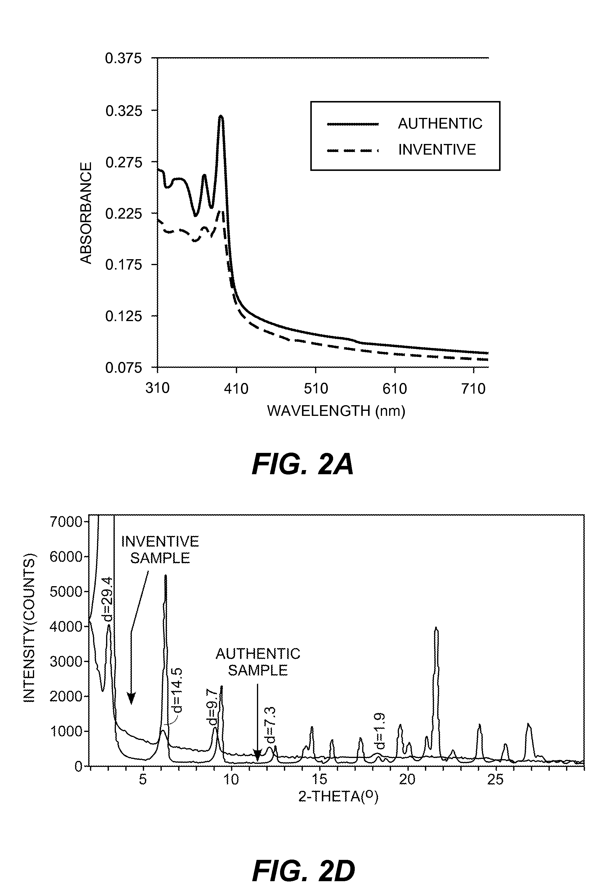
[0261]A 2 wt. % solution of 1,5-naphthalenedicarboxylic acid-4,8-bis[(dodecylmino)carbonyl] in dimethylacetamide was drop cast onto a glass plate and solvent evaporated to form an article with the coated amic acid precursor. Absorption spectrum was recorded and the plate was heated at 180° C. for 20 minutes. Absorption spectrum after heating clearly shows the t...

invention example 2

Preparation of 1,5-naphthalenedicarboxylic acid-4,8-bis[(cyclopentylamino)carbonyl]

[0263]

[0264]Freshly sublimed 1,4,5,8-napthalene tetracarboxylic acid dianhydride (44 mg, 0.16 mmol) was added to dimethylacetamide (2 ml) and sonicated for 5 minutes to form a slightly cloudy dispersion. A solution of cyclopentylamine (28 mg; 0.32 mmol) in dimethylacetamide (1 ml) was slowly added to the dispersion to obtain a clear pale yellow solution. Solvent removed under reduced pressure to obtain a solid. 1H and 13C NMR and of the product were consistent with assigned structure. 1H NMR and IR spectra of the product were consistent with assigned structure.

Conversion of 1,5-naphthalenedicarboxylic acid-4,8-bis[(cyclopentylamino)carbonyl] to N,N′-bis(cyclopentyl)naphthalene diimide in Solid State

[0265]

[0266]A 2 wt. % solution of 1,5-naphthalenedicarboxylic acid-4,8-bis[(cyclopentyl)carbonyl] was spin coated onto a glass plate at 800 RPM to form an article coated with an amic acid precursor. The gla...

invention example 3

Thin Film Device Preparation

OTFT Test Device Preparation Employing Arylene Diimide Generated in Thin Solid Film from Amic Acid Precursor

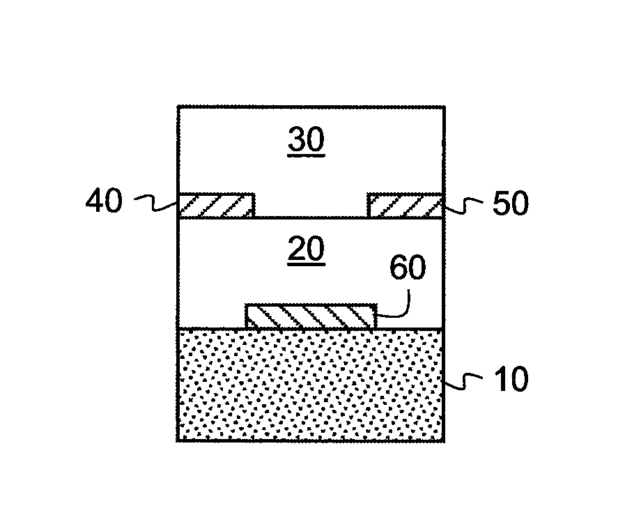
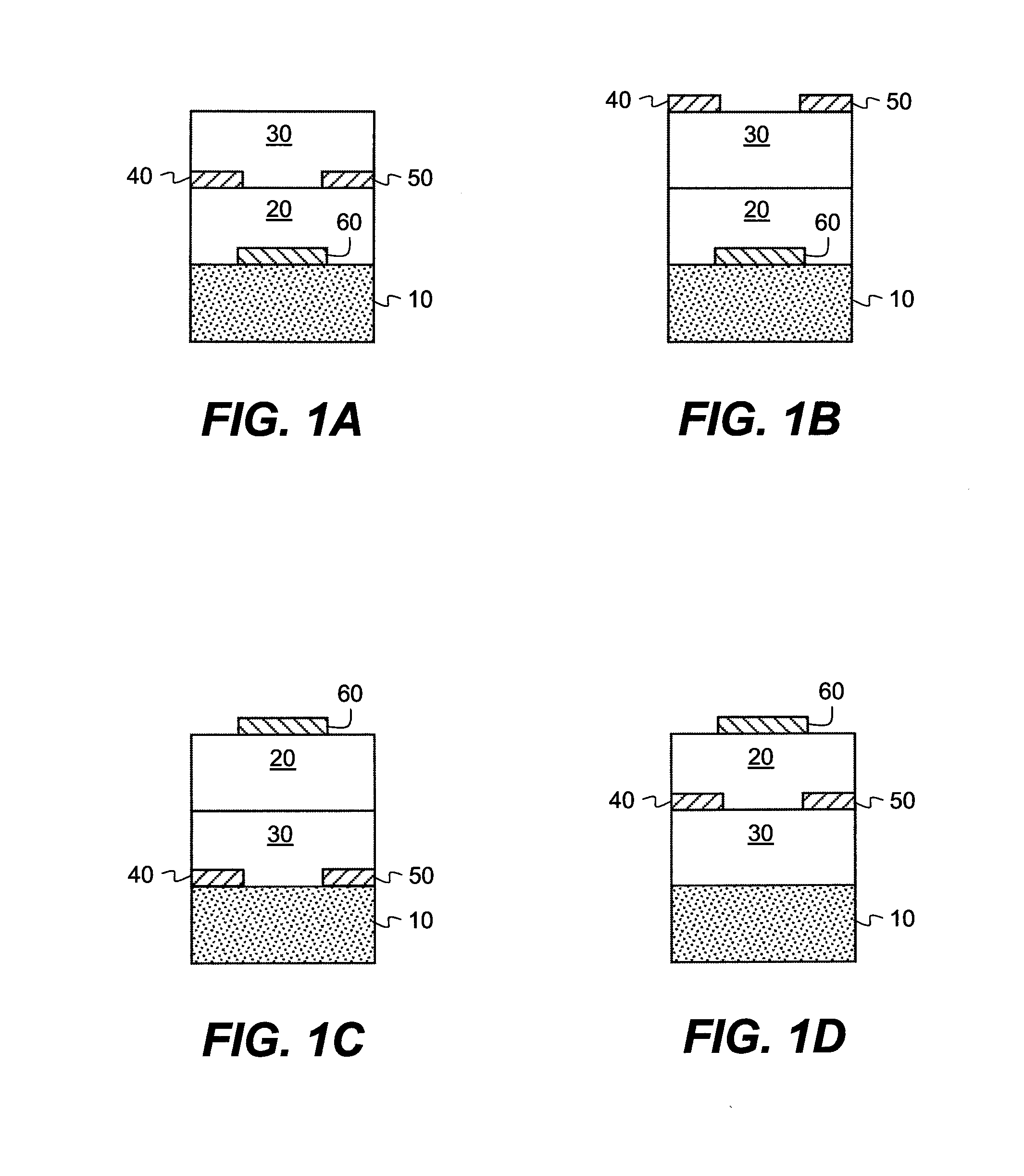
[0268]In order to test the electrical characteristics of the semiconductive material, field-effect transistors were made using the top-contact geometry described above. The substrate was a heavily doped silicon wafer, which also served as the gate electrode of the transistor. The gate dielectric was a thermally grown SiO2 layer with a thickness of 190 nm. The wafer was cleaned for 10 minutes in a piranah solution, followed by a 6-minute exposure in a UV / ozone chamber. The cleaned surface was then treated with a self-assembled monolayer of octadecyltrichlorosilane (OTS), made from a heptane solution under a humidity-controlled environment. Water contact angles and layer thickness were measured to ensure the quality of the treated surface. Surfaces with a good quality OTS layer have water contact angles >90° and a thickness determined from ellipsometr...


PUM


Abstract

An amic acid or amic ester precursor can be applied to a substrate and thermally converted into a semiconducting layer of the corresponding arylene diimide. This semiconducting thin film can be used in various articles including thin-film transistor devices that can be incorporated into a variety of electronic devices. In this manner, the arylene diimide need not be coated but is generated in situ from a solvent-soluble, easily coated precursor compound.

Description

FIELD OF THE INVENTION[0001]This invention relates to methods of preparing thin films of arylene diimide compounds as organic semiconductor layers. The arylene diimide compounds can be derived by providing thin films of a unique class of amic acid or amic ester precursors that are then thermally converted to the corresponding arylene diimide. The invention also provides methods for providing precursors that can be converted to the arylene diimides.BACKGROUND OF THE INVENTION[0002]Thin film transistors (“TFT's”) are widely used as switching elements in electronics, for example, in active-matrix liquid-crystal displays, smart cards, and a variety of other electronic devices and components thereof. The thin film transistor (TFT) is an example of a field effect transistor (“FET”). The best-known example of an FET is the “MOSFET (Metal-Oxide-Semiconductor-FET) that can be used for high-speed applications. Most thin film devices are made using amorphous silicon as the semiconductor becaus...

Claims


Application Information

Patent Timeline
Patent Type & Authority Patents(United States)
IPC IPC(8): H01L51/40C07C229/00H01L21/00
CPCH01L51/0053H01L51/0003H01L51/0541H01L51/0545C09B5/62C09B57/08H10K71/12H10K85/621H10K10/464H10K10/466
Inventor SHUKLA, DEEPAKMEYER, DIANNE M.AHEARN, WENDY G.
Owner EASTMAN KODAK CO
Why Eureka
Try Eureka